Array substrate and manufacturing method thereof

A technology of an array substrate and a manufacturing method, which is applied to the array substrate and the manufacturing field thereof, can solve problems such as copper oxidation, and achieve the effects of preventing copper oxidation, reducing damage, and avoiding diffusion

Inactive Publication Date: 2019-11-29
SHENZHEN CHINA STAR OPTOELECTRONICS SEMICON DISPLAY TECH CO LTD
View PDF5 Cites 10 Cited by
  • Summary
  • Abstract
  • Description
  • Claims
  • Application Information

AI Technical Summary

Problems solved by technology

[0002] The metal oxide thin film transistor (Oxide TFT) backplane with a top gate self-aligned structure, the light-shielding layer uses copper (Cu) to reduce the risk of routing other metal layers, but copper will have oxidation problems

Method used


Image

  • Array substrate and manufacturing method thereof
  • Array substrate and manufacturing method thereof
  • Array substrate and manufacturing method thereof

Examples


Embodiment Construction

[0018] The following descriptions of the various embodiments refer to the accompanying drawings to illustrate specific embodiments in which the present invention can be practiced. The directional terms mentioned in the present invention, such as "up", "down", "front", "back", "left", "right", "top", "bottom", "horizontal", "vertical", etc. , are for orientation only with reference to the attached drawings. Therefore, the directional terms used are used to illustrate and understand the present invention, but not to limit the present invention.

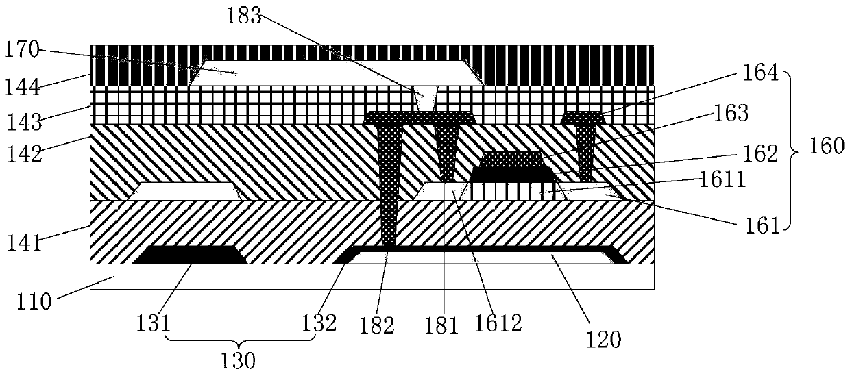
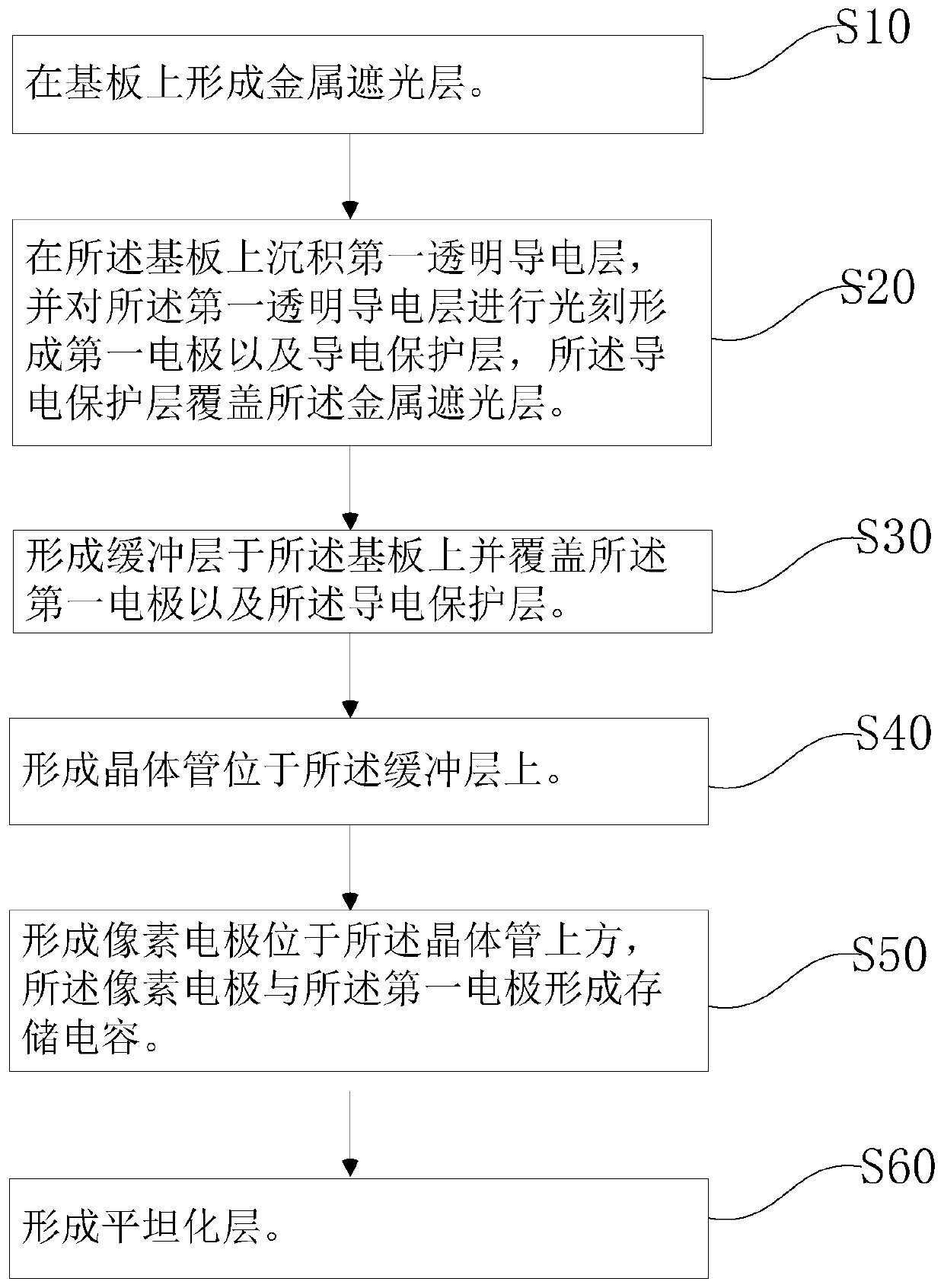
[0019] see figure 1 The present invention provides an array substrate 10 comprising a substrate 110, a metal light-shielding layer 120, a first electrode 131, a conductive protection layer 132, a buffer layer 141, a transistor 160, an interlayer insulating layer 142, a passivation layer 143, and a pixel electrode 170 and a planarization layer 144 .

[0020] The material of the metal light-shielding layer 120 is an alloy of one or mor...


PUM

PropertyMeasurementUnit
thicknessaaaaaaaaaa
thicknessaaaaaaaaaa
thicknessaaaaaaaaaa

Abstract

An array substrate comprises a substrate body, a metal shading layer, a conductive protection layer, a buffer layer, a transistor and a pixel electrode. The conductive protection layer covers the metal shading layer. The buffer layer is located on the substrate and covers the conductive protective layer. The transistor is located on the buffer layer and connected with the conductive protective layer. The pixel electrode is connected with the transistor. The problem of copper oxidation of the metal oxide thin film transistor driving backboard is effectively solved, and the transparent conductive layer covers the surface of the shading layer copper to form protection for copper, thereby preventing copper oxidation, avoiding copper diffusion, reducing damage of etching to copper and reducingthe risk of copper stripping of the shading layer.

Description

technical field [0001] The invention relates to the field of display technology, in particular to an array substrate and a manufacturing method thereof. Background technique [0002] For the metal oxide thin film transistor (Oxide TFT) backplane of the top gate self-aligned structure, copper (Cu) is used for the light-shielding layer to reduce the risk of routing other metal layers, but copper will have oxidation problems. Contents of the invention [0003] In view of this, the object of the present invention is to provide an array substrate and its manufacturing method, so as to solve the problems in the prior art. [0004] The technical solution of the present invention provides an array substrate and its manufacturing method. The array substrate includes: a substrate; a metal light-shielding layer located on the substrate; a conductive protective layer covering the metal light-shielding layer; a buffer layer located on the The substrate is on and covers the conductive ...

Claims


Application Information

Patent Timeline
Patent Type & Authority Applications(China)
IPC IPC(8): H01L27/12H01L21/77
CPCH01L27/124H01L27/1244H01L27/1259H01L27/1225H01L29/7869H01L29/78633H01L27/1255H01L27/1237H01L27/1262
Inventor 周星宇林振国徐源竣吕伯彦
Owner SHENZHEN CHINA STAR OPTOELECTRONICS SEMICON DISPLAY TECH CO LTD
Why Eureka
Try Eureka