
Semiconductor device and manufacturing method thereof
A semiconductor and device technology, applied in the field of power semiconductor devices, can solve problems such as low breakdown voltage and low constant current value, achieve high withstand voltage, improve dynamic impedance value, and excellent constant current characteristics
- Summary
- Abstract
- Description
- Claims
- Application Information
AI Technical Summary
Problems solved by technology
Method used
Image

Examples
Embodiment Construction
[0044] The principles and features of the present invention are described below in conjunction with the accompanying drawings, and the examples given are only used to explain the present invention, and are not intended to limit the scope of the present invention.
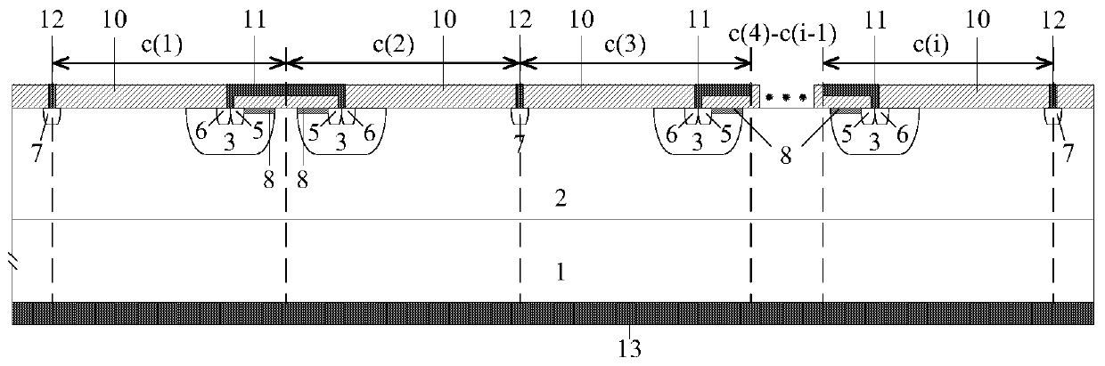
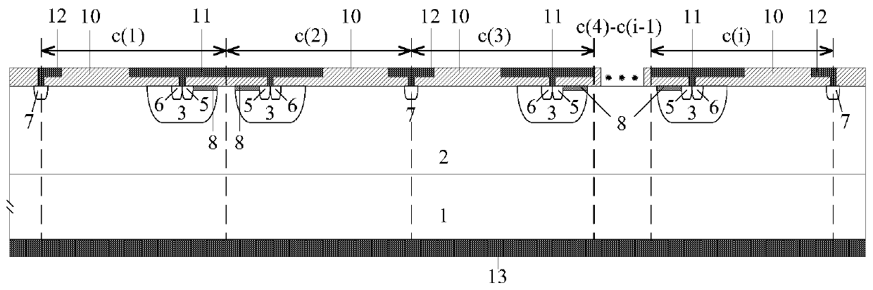
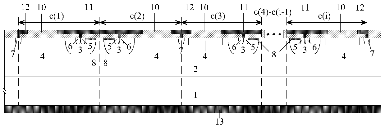
[0045] As shown in Figure 1(a), a semiconductor device provided by the first embodiment of the present invention is formed by connecting multiple cells with the same structure in an interdigitated manner, and the cell structure includes a second conductivity type lightly doped Substrate 1, first conductivity type lightly doped epitaxial layer 2, oxide medium layer 10, metal cathode 11, metal anode 12 and back metal electrode 13; the first conductivity type lightly doped epitaxial layer 2 has diffused second conductivity type The well region 3, the first conductivity type depletion channel region 8, the first heavily doped region 5, the second heavily doped region 6 and the third heavily doped region 7, the first heavil...
PUM
 Abstract
Description
Claims
Application Information