Method for direct patterned growth of atomic layer transition metal dichalcogenides

A transition metal dichalcogenide, transition metal technology, applied in metal selenide/telluride, chemical instruments and methods, molybdenum sulfide, etc., can solve problems such as changing the inherent properties of TMD monolayers, mask resolution, and complexity

Active Publication Date: 2022-04-05
HONDA MOTOR CO LTD
View PDF7 Cites 0 Cited by
  • Summary
  • Abstract
  • Description
  • Claims
  • Application Information

AI Technical Summary

Problems solved by technology

However, utilizing photolithographic processes is complicated because not only mask resolution issues but also the required reactive ion etching can inadvertently alter the intrinsic properties of TMD monolayers.
Therefore, a continuing challenge for these materials lies not only in the synthesis of large monolayer domains but also in controlling their growth patterns according to circuit design.

Method used


Image

  • Method for direct patterned growth of atomic layer transition metal dichalcogenides
  • Method for direct patterned growth of atomic layer transition metal dichalcogenides
  • Method for direct patterned growth of atomic layer transition metal dichalcogenides

Examples


Embodiment Construction

[0011] The detailed description set forth below in connection with the accompanying drawings is intended as a description of various configurations and is not intended to represent the only configurations in which the concepts described herein may be practiced. The detailed description includes specific details for the purpose of providing a thorough understanding of various concepts. It will be apparent, however, to one skilled in the art that these concepts may be practiced without these specific details.

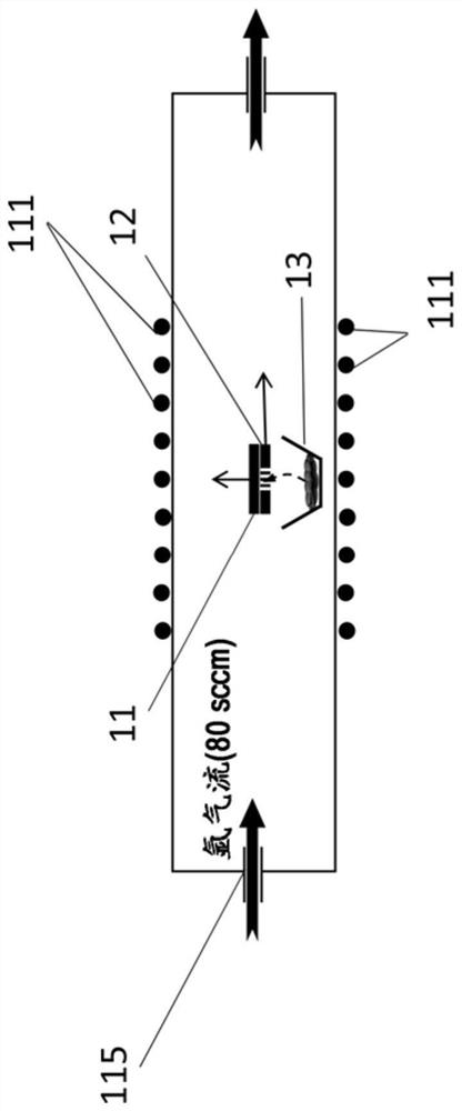
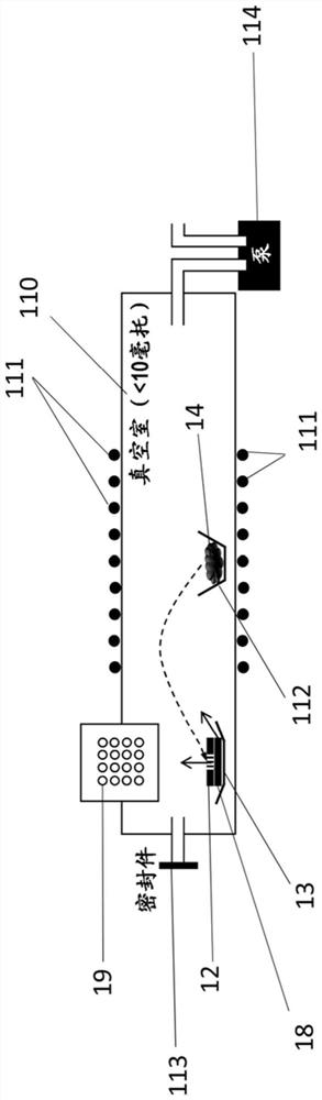
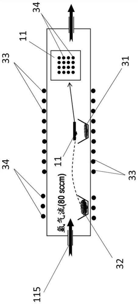
[0012] This disclosure describes a newly developed method for molybdenum disulfide (MoS 2 ) and / or direct patterned growth of atomic layers of other transition metal dichalcogenide materials. Patterned growth has been achieved by using salts as intermediate or template materials. Specifically, the salt can be deposited on the substrate through a mask having a desired pattern. The method leads to atomic layer MoS 2 (or other metal dichalcogenide materials) of the same ...


PUM

PropertyMeasurementUnit
sizeaaaaaaaaaa
thicknessaaaaaaaaaa
diameteraaaaaaaaaa

Abstract

A method of direct growth of a patterned transition metal dichalcogenide monolayer, the method comprising the steps of: providing a substrate covered by a mask having a pattern defined by one or more shaped holes; or a plurality of shaped holes thermally depositing the salt on the substrate so that the deposition salt is arranged on the substrate in a mask pattern; and thermally co-depositing the transition metal oxide and the chalcogen element onto the deposition salt to form Graphical patterning of transition metal dichalcogenide monolayers. Also provided are patterned transition metal dichalcogenide monolayers prepared according to the method.

Description

[0001] Cross References to Related Applications [0002] This application claims priority to U.S. Provisional Application No. 62 / 678802, filed May 31, 2018. The disclosure of this priority application is incorporated herein by reference in its entirety. Background technique [0003] Atomic layer transition metal dichalcogenides (TMDs) have been the subject of intensive research due to their promising optoelectronic and catalytic properties as well as next-generation circuits. Using TMDs in circuits not only needs to maintain low contact resistance with single-layer materials, but also needs to be compatible with very fine photolithographic processes with the necessary patterning. However, utilizing photolithographic processes is complicated by not only mask resolution issues but also the required reactive ion etching that may inadvertently alter the intrinsic properties of TMD monolayers. Thus, a continuing challenge for these materials lies not only in the synthesis of lar...

Claims


Application Information

Patent Timeline
Patent Type & Authority Patents(China)
IPC IPC(8): C23C16/04C23C16/30C23C16/455
CPCC23C16/042C23C16/305C23C16/45525C23C16/4481C23C14/042C23C14/0694C23C14/24C23C16/04C23C16/4488H01L21/02645H01L21/02568H01L21/02439H01L21/02488H01L21/02381H01L21/02502H01L21/02631H01L21/0262C01G39/06B82Y40/00C01G41/00C01P2004/03C01P2002/82C01B19/007H01L21/02639H01L29/24
Inventor 李煦凡A·哈鲁特尤亚恩
Owner HONDA MOTOR CO LTD
Why Eureka
Try Eureka