Multideposition SACVD reactor

a chemical vapor deposition and reactor technology, applied in chemical vapor deposition coating, coating, metallic material coating process, etc., can solve the problems of inability to deposit sisub>3/sub>n, time-consuming operation, and device density and complexity increase, and achieve the effect of rapid thermal deposition of dielectric materials

Inactive Publication Date: 2005-10-20
RAFFIN PATRICK +4
View PDF8 Cites 5 Cited by
  • Summary
  • Abstract
  • Description
  • Claims
  • Application Information

AI Technical Summary

Benefits of technology

[0036] It is therefore a primary object of the present invention to provide a multideposition CVD reactor enabling the rapid thermal deposition of di

Problems solved by technology

Foreign elements that are incorporated into the deposited films during fabrication also drive device performance, and thus are becoming more important to date, as devices become more and more dense and complex.
As a whole

Method used


Image

  • Multideposition SACVD reactor
  • Multideposition SACVD reactor
  • Multideposition SACVD reactor

Examples


Embodiment Construction

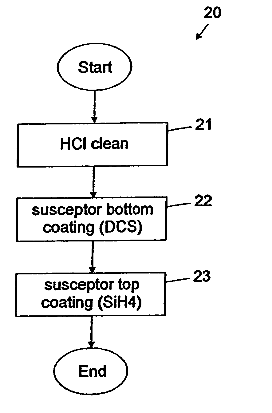
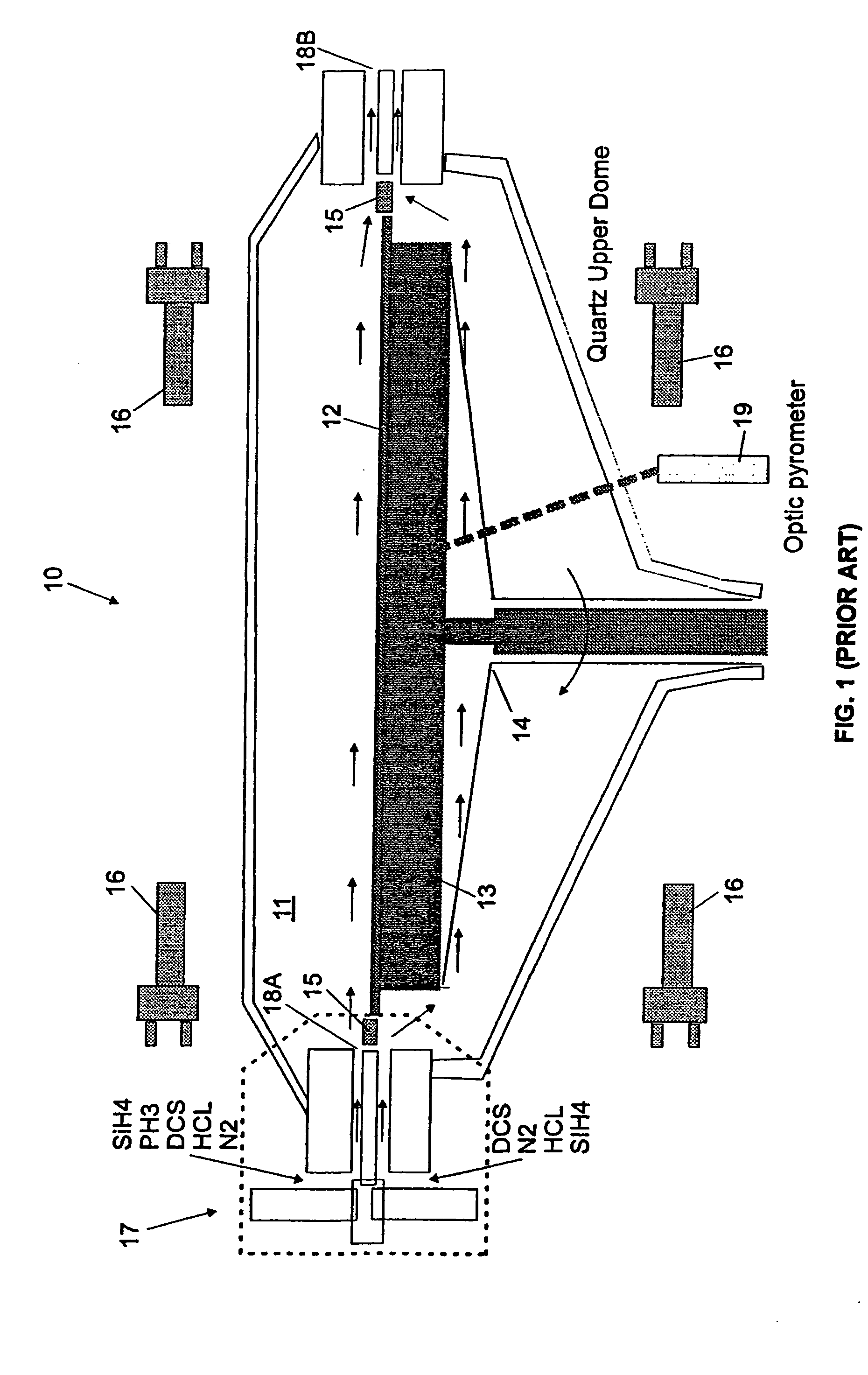
[0055] Historically, LPCVD processes have been performed in vertical furnaces. In the past several years, new deposition tools have become available which overcome the limitations of vertical furnaces because they are single-wafer processing based systems. The SACVD Centura HTF reactor is a good example of that new generation of deposition equipments. However, it is strictly limited to the deposition of polysilicon films. It is a cold-wall reactor that uses radiant heating for thermal energy. It operates at reduced pressure and in a temperature range of 550-1200° C. (depending upon the type of operation: deposition or cleaning). FIG. 1 schematically shows the cross-section of the SACVD Centura reactor with its major elements. Now tuning to FIG. 1, reactor 10 has top and bottom walls (dome), side walls and a bottom wall that define the internal volume of the processing vacuum chamber 11 into which a substrate, typically a silicon wafer 12, can be loaded. The wafer 12 sits on a carbon...


PUM

PropertyMeasurementUnit
Temperatureaaaaaaaaaa
Thicknessaaaaaaaaaa

Abstract

There is disclosed a high throughput multideposition SACVD reactor that enables the rapid thermal deposition of dielectric materials such as Si3N4, SiO2, and SiON and non-&electric materials such as polysilicon onto a semiconductor substrate in the same chamber according to the desired sequence. Such a reactor has a processing chamber which is well adapted to single semiconductor wafer processing. The processing chamber includes an improved susceptor to support the wafer and a specific gas distribution system adapted to supply the different gases used in the deposition process and for cleaning. The improved susceptor consists of a standard carbon plate coated with a polysilicon film to protect it against said cleaning gases when they are aggressive to carbon. The present invention also encompasses a method of fabricating said improved susceptor.

Description

FIELD OF THE INVENTION [0001] The present invention relates to the manufacture of semiconductor integrated circuits (ICs) and more particularly to a multideposition sub-atmospheric chemical vapor deposition (SACVD) reactor enabling the rapid thermal deposition of dielectric materials such Si3N4, SiO2, and SiON and of non-dielectric materials such as polysilicon onto a substrate. According to the present invention, said dielectric / non-dielectric materials can be now deposited according to the desired sequence in the same chamber of the multideposition SACVD reactor, significantly reducing cycle time, total thermal budget and pattern factor effects. BACKGROUND OF TE INVENTION [0002] Short cycle time and low thermal budget are certainly the most critical points for Application Specific Integrated Circuit (ASIC) and Dynamic Random Access Memory (DRAM) products manufacturing respectively. The continuous technical progress in the last decades has resulted in the emergence of new technique...

Claims


Application Information

Patent Timeline
IPC IPC(8): C23C16/44H01L21/302C23C16/455C23C16/458C23C16/54H01L21/205H01L21/285H01L21/3065H01L21/31H01L21/314H01L21/316H01L21/318
CPCC23C16/4405C23C16/45561C23C16/45574C23C16/4581C23C16/54H01L21/3185H01L21/28525H01L21/28556H01L21/3144H01L21/3145H01L21/31612H01L21/28518H01L21/02271H01L21/02211H01L21/0217H01L21/02164H01L21/0214
Inventor RAFFIN, PATRICKDELARUE, FABRICEWAECHTER, JEAN MARCBALSAN, CHRISTOPHEJOURNE, JOEL
Owner RAFFIN PATRICK
Why Eureka
Try Eureka