Perovskite film solar cell and preparation method thereof

A solar cell and perovskite technology, applied in circuits, photovoltaic power generation, electrical components, etc., can solve the problems of low electron transmission performance, affecting the photocurrent output of the device, affecting the overall efficiency of the device, etc., and achieve the effect of reducing costs

Active Publication Date: 2017-12-01
SUZHOU INST OF NANO TECH & NANO BIONICS CHINESE ACEDEMY OF SCI
View PDF3 Cites 5 Cited by
  • Summary
  • Abstract
  • Description
  • Claims
  • Application Information

AI Technical Summary

Problems solved by technology

but since C 60 Electron transport performance is lower than that of PC 61 BM, using C 60 As an electron transport layer, it will affect the photocurrent output of the device, and then affect the overall efficiency of the device.

Method used


Image

  • Perovskite film solar cell and preparation method thereof
  • Perovskite film solar cell and preparation method thereof
  • Perovskite film solar cell and preparation method thereof

Examples


preparation example Construction

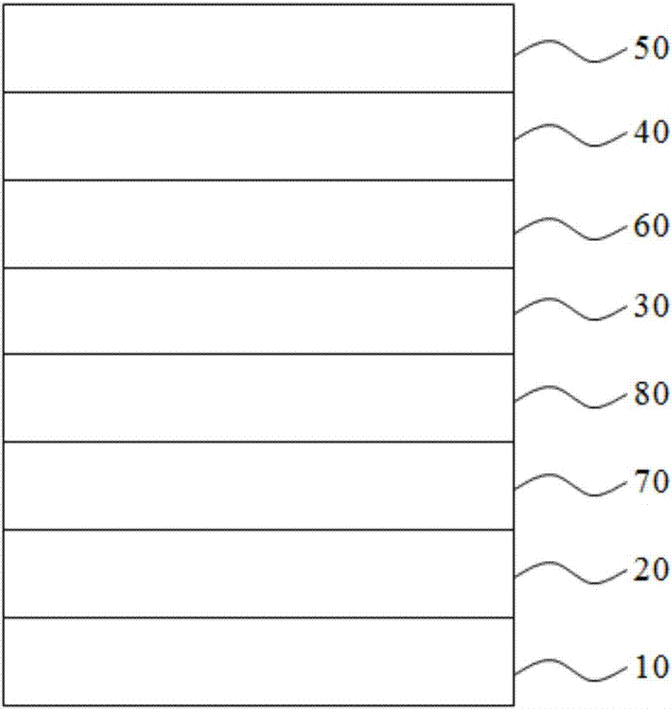
[0038] see below figure 1 The preparation method of the perovskite thin film solar cell described above is described in detail, and the method comprises steps:

[0039] S1 , providing a substrate 10 and preparing and forming a first electrode 20 on the substrate 10 .

[0040] S2 , preparing and forming a hole transport layer 70 on the first electrode 20 . Specifically, the hole transport layer 70 can be prepared by a spin coating method. For example, the solution of the material used to prepare the hole transport layer 70 is spin-coated to form a film, and then annealed on a hot plate to form the hole transport layer 70 . Commonly used, the aqueous solution of PEDOT:PSS is spin-coated and then fired at a temperature of 80-140°C for 10-30 minutes.

[0041] S3 , preparing and forming an interface modification layer 80 on the hole transport layer 70 . Specifically, the interface modification layer 80 can be prepared by a spin coating method. For example, the solution of the ...
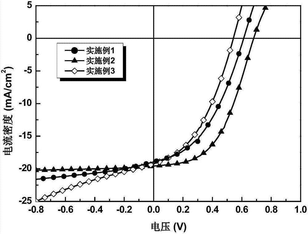
Embodiment 1

[0050] This example selects a single specific material, does not limit the selection of other materials, but only exemplifies the invention.

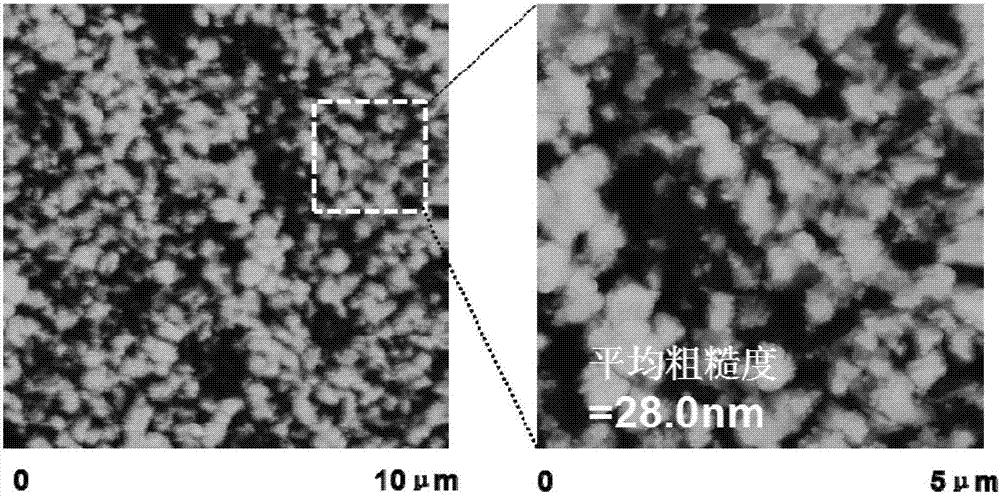
[0051] (1) Clean the glass substrate 10 with the ITO electrode (the first electrode 20 ) with acetone, ethanol, and isopropanol in sequence for 30 minutes, then dry the substrate with nitrogen gas, and then treat it with ultraviolet light for 30 minutes.

[0052] (2) Spin-coat PEDOT:PSS (4083), the material of the hole transport layer, on the dried glass substrate 10 after ultraviolet treatment, at a rotation speed of 3500 rpm, and rotate for 60 seconds to obtain a layer of uniform PEDOT:PSS film. Subsequently, the PEDOT:PSS thin film was fired in air at 125° C. for 10 minutes, and then cooled to room temperature to form the hole transport layer 70 .

[0053] (3), use 2wt% PSSNa polymer aqueous solution, spin-coat on the hole transport layer 70, the rotation speed is 2000 rpm, the time is 60 seconds, put it in the glove box after 5 minu...

Embodiment 2

[0059] The thickness control of the second electron transport layer 60 in the step (5) in embodiment 1 is 90nm, the thickness control of the first electron transport layer 40 in the step (6) is 90nm, and other conditions are the same preparation as in embodiment 1 Perovskite thin film solar cells.


PUM


Abstract

The invention discloses a perovskite film solar cell comprising a first electrode; a perovskite light-absorbing layer which is arranged on the first electrode; a first electron transmission layer which is arranged on the perovskite light-absorbing layer; and a second electrode which is arranged on the first electron transmission layer, wherein the material of the first electron transmission layer is C60 doped with the organic micromolecule dopant. The preparation method of the solar cell comprises the steps that the organic micromolecule dopant and the C60 are deposited after evaporation by applying the double source vacuum thermal deposition technology, and the first electron transmission layer is prepared and formed on the perovskite light-absorbing layer. The C60 doped with the organic micromolecule dopant is used as the electron transmission layer so that the requirement of photocurrent output of the device can be met, the cost of the device can also be greatly reduced and thus industrial popularization and application of the perovskite film solar cell are facilitated.

Description

technical field [0001] The invention relates to the technical field of photoelectric functional materials and devices, in particular to a perovskite thin-film solar cell and a preparation method thereof. Background technique [0002] Organic-inorganic hybrid perovskite solar electronics have attracted widespread attention because of their solution processing, low energy consumption in the preparation process and high device efficiency. Especially in terms of device efficiency, the device efficiency of single-junction perovskite solar cells has exceeded 20% so far. With the improvement of device efficiency, the structure of the device is also gradually evolving, from the mesoporous structure similar to the structure of the dye-sensitized cell, to the planar heterojunction structure and the trans-planar heterojunction structure with a dense electron transport layer. [0003] Among them, the trans planar heterojunction structure battery includes a transparent bottom electrode,...

Claims


Application Information

Patent Timeline
Patent Type & Authority Applications(China)
IPC IPC(8): H01L51/42H01L51/46H01L51/48
CPCH10K71/164H10K85/211H10K30/10Y02E10/549
Inventor 李雪原张连萍马昌期
Owner SUZHOU INST OF NANO TECH & NANO BIONICS CHINESE ACEDEMY OF SCI
Why Eureka
Try Eureka