Method for manufacturing metal gate and method for manufacturing semiconductor device

A metal gate and manufacturing method technology, applied in semiconductor/solid-state device manufacturing, semiconductor devices, electrical components and other directions, can solve problems such as affecting device performance, easy to generate voids, gaps, etc., to improve performance, improve gap filling capability, Reduce the effect of filling voids

Active Publication Date: 2019-12-13
SEMICON MFG INT (SHANGHAI) CORP +1
View PDF4 Cites 3 Cited by
  • Summary
  • Abstract
  • Description
  • Claims
  • Application Information

AI Technical Summary

Problems solved by technology

However, at the new process technology node below 28nm, the size of the gate is gradually reduced, and the aspect ratio (Aspect Ratio) in the gate trench is gradually increased, which affects the gap filling of the high-K metal gate, and is prone to voids (Void) or Defects such as seams seriously affect the improvement of device performance

Method used


Image

  • Method for manufacturing metal gate and method for manufacturing semiconductor device
  • Method for manufacturing metal gate and method for manufacturing semiconductor device
  • Method for manufacturing metal gate and method for manufacturing semiconductor device

Examples


Embodiment Construction

[0036] A method for manufacturing a high-K metal gate, comprising the following steps:

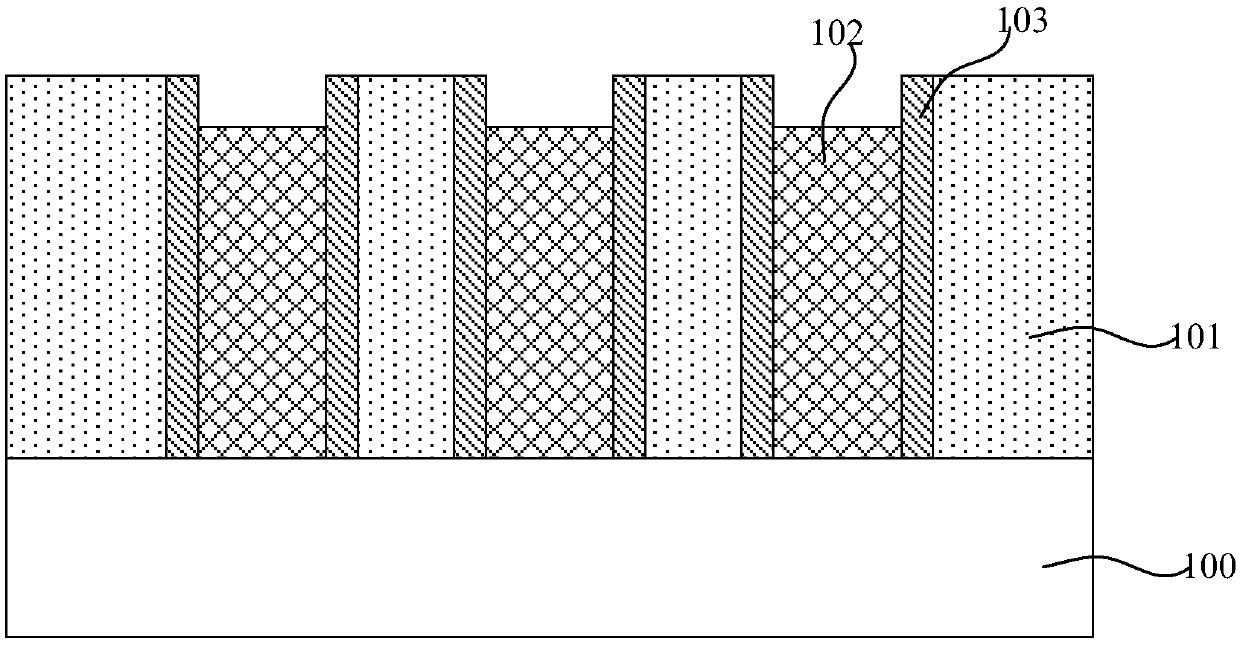
[0037] First, please refer to Figure 1A , providing a semiconductor substrate 100, forming a polysilicon gate 102 on the semiconductor substrate 100 as a dummy gate replaced by a subsequent metal gate, and forming sidewalls 103 on the sidewall of the polysilicon gate 102;

[0038] Next, please continue to refer to Figure 1A , depositing an interlayer dielectric layer 101, and performing chemical mechanical planarization on the top of the deposited interlayer dielectric layer 101 until the top surface of the polysilicon gate 102 is exposed;

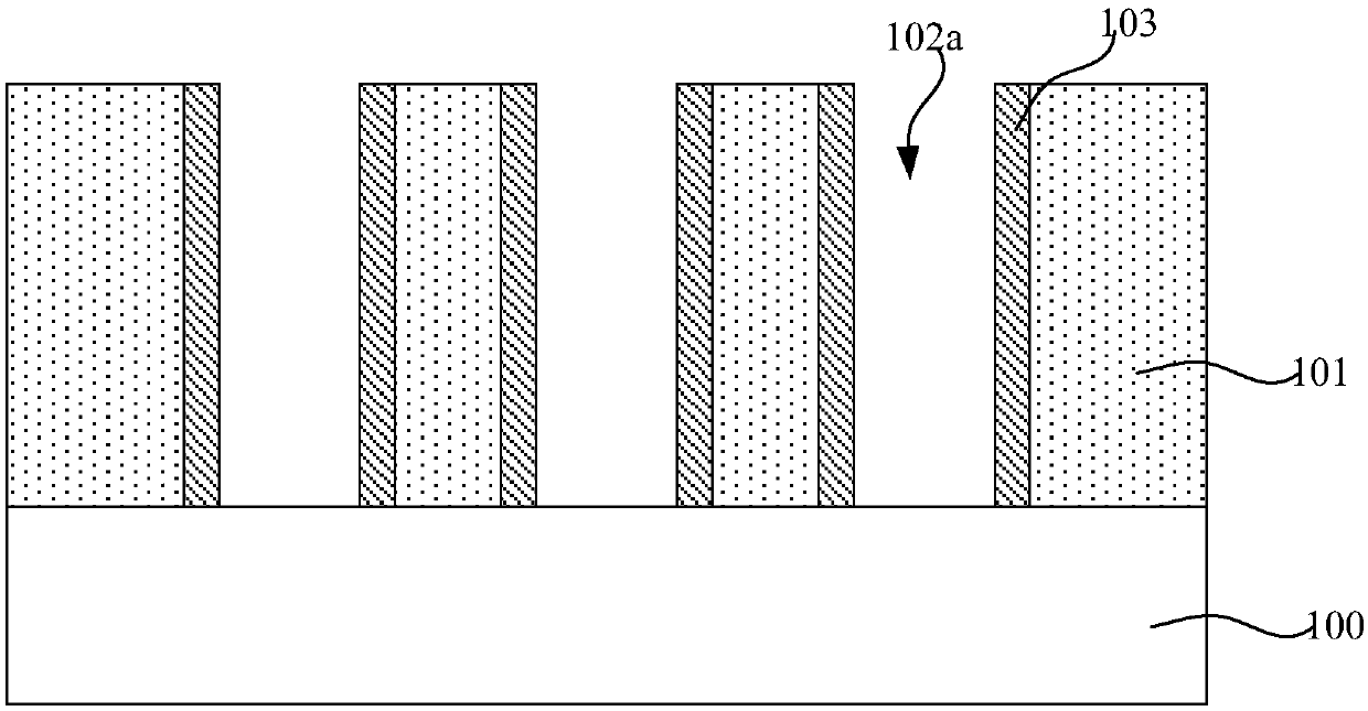
[0039] Then, refer to Figure 1A and Figure 1B , first using a dry etching process to partially etch the exposed polysilicon gate 102 to provide an etching solution storage area for subsequent wet etching to improve the effect of subsequent wet etching; then use tetramethyl Ammonium hydroxide solution (THMA) completely removes the remaining poly...


PUM


Abstract

The invention provides a method for manufacturing a metal gate and a method for manufacturing a semiconductor device. Before a dummy gate is removed to form an opening for filling metal gate, a portion of an initial spacer on the sidewall of the dummy gate is firstly subjected to material modification in order that the initial spacer is transformed into a first spacer not subjected to material modification and a second spacer located on the first spacer and subjected to material modification. Thus, all or part of the second spacer can be removed simultaneously while the virtual gate is removed, so that the opening having an wide top and a narrow bottom and for filling the metal gate can be formed after the process of removing the virtual gate ends. The depth-to-width ratio of the opening is reduced so as to improve the subsequent gap filling capability of the metal gate, and reduce defects such as filling voids and gaps of the metal gate, thereby improving the performance of the finally manufactured semiconductor device.

Description

technical field [0001] The invention relates to the technical field of integrated circuit manufacturing, in particular to a method for manufacturing a metal gate and a method for manufacturing a semiconductor device. Background technique [0002] With the continuous improvement of the integration of semiconductor devices, when making MOS transistors, high-K metal gates with high-K (dielectric constant K greater than or equal to 10) materials as gate dielectric layers and metal materials as gate electrodes have become semiconductor devices. The mainstream technology for manufacturing 32nm and below processes, and currently it is mostly manufactured by the Gate-last process. The Gate-last process is a replacement metal gate process (Replacement Metal Gate), usually using the traditional polysilicon gate The dummy polysilicon gate (Dummy Poly Gate, also known as dummy gate or sacrificial gate) is manufactured by the electrode process, and after the high-temperature annealing tr...

Claims


Application Information

Patent Timeline
Patent Type & Authority Applications(China)
IPC IPC(8): H01L21/28H01L21/336
CPCH01L29/401H01L29/66477H01L29/66545H01L29/66795
Inventor 纪世良张海洋
Owner SEMICON MFG INT (SHANGHAI) CORP
Why Eureka
Try Eureka