Manufacturing method of organic el display

A manufacturing method and display technology, applied in semiconductor/solid-state device manufacturing, instruments, electric solid-state devices, etc., can solve the problems of reducing the thickness of stretched films and not being able to obtain enough thin sheets, and achieve the effect of enhancing thinning and flexibility

Active Publication Date: 2022-04-19
TOKYO ELECTRON LTD
View PDF14 Cites 0 Cited by
  • Summary
  • Abstract
  • Description
  • Claims
  • Application Information

AI Technical Summary

Problems solved by technology

However, when a stretched film is used in the production of a polarizing plate and a wavelength plate as in the prior art, there is a limit to reducing the film thickness of the stretched film itself, and a sufficiently thin sheet cannot be obtained.

Method used


Image

  • Manufacturing method of organic el display
  • Manufacturing method of organic el display
  • Manufacturing method of organic el display

Examples


Embodiment Construction

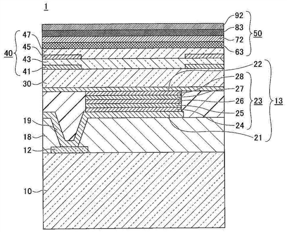
[0054] Hereinafter, embodiments for carrying out the present invention will be described with reference to the drawings. In each drawing, the same or corresponding reference numerals are assigned to the same or corresponding structures, and description thereof will be omitted.

[0055]

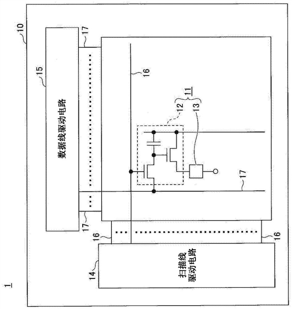
[0056] figure 1 It is a top view showing an organic EL display according to one embodiment. exist figure 1 In , the circuit of one unit circuit 11 is enlarged and shown.

[0057] The organic EL display 1 includes a substrate 10 , a plurality of unit circuits 11 arranged on the substrate 10 , a scanning line driving circuit 14 disposed on the substrate 10 , and a data line driving circuit 15 disposed on the substrate 10 . The unit circuit 11 is provided in an area surrounded by a plurality of scanning lines 16 connected to the scanning line driving circuit 14 and a plurality of data lines 17 connected to the data line driving circuit 15 . The unit circuit 11 includes a TFT layer 12 and an...


PUM


Abstract

A method for manufacturing an organic EL display, comprising an optical member forming step of applying an optical film coating liquid containing liquid crystal molecules and a solvent on a substrate on which an organic light emitting diode has been preformed and drying the optical member, To form an optical film with liquid crystal molecules aligned.

Description

technical field [0001] The invention relates to a method for manufacturing an organic EL display. Background technique [0002] For example, in a display using an organic light emitting diode (OLED: Organic Light Emitting Diode) (hereinafter also referred to as an "organic EL (Electro Luminescence) display"), a circular polarizing plate is used to suppress external light reflection. The circular polarizing plate is produced by laminating a linear polarizing plate and a wavelength plate (retardation plate) so that their polarization axes cross at 45 degrees. [0003] Also, for example, the wavelength plate may be formed only so that its polarization axis is inclined by 15 degrees or 75 degrees. Therefore, it is necessary to form polarizing plates and wavelength plates at arbitrary angles. In addition, in order to make the polarization axes of the polarizing plate and the wavelength plate intersect at an arbitrary angle, it is necessary to form the polarizing plate and the w...

Claims


Application Information

Patent Timeline
Patent Type & Authority Patents(China)
IPC IPC(8): H01L51/52
CPCH05B33/02H05B33/10G02B5/30G09F9/00G09F9/30H10K59/00H10K50/00G02B5/3025G02B5/3083H10K59/50H10K71/231H10K71/12H10K50/85H10K71/00
Inventor 池田文彦
Owner TOKYO ELECTRON LTD
Why Eureka
Try Eureka