Bidirectional thyristor and electronic product
A bidirectional thyristor, carrier technology, applied in the direction of circuits, electrical components, semiconductor devices, etc., can solve the problems of thyristor surge capacity reduction, large capacitance, product restrictions, etc., to reduce concentration, reduce overshoot voltage, and large discharge effect of space
- Summary
- Abstract
- Description
- Claims
- Application Information
AI Technical Summary
Problems solved by technology
Method used
Image
Examples
Embodiment 1
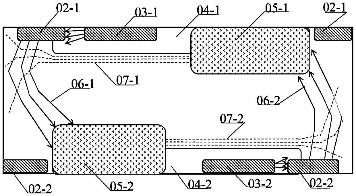
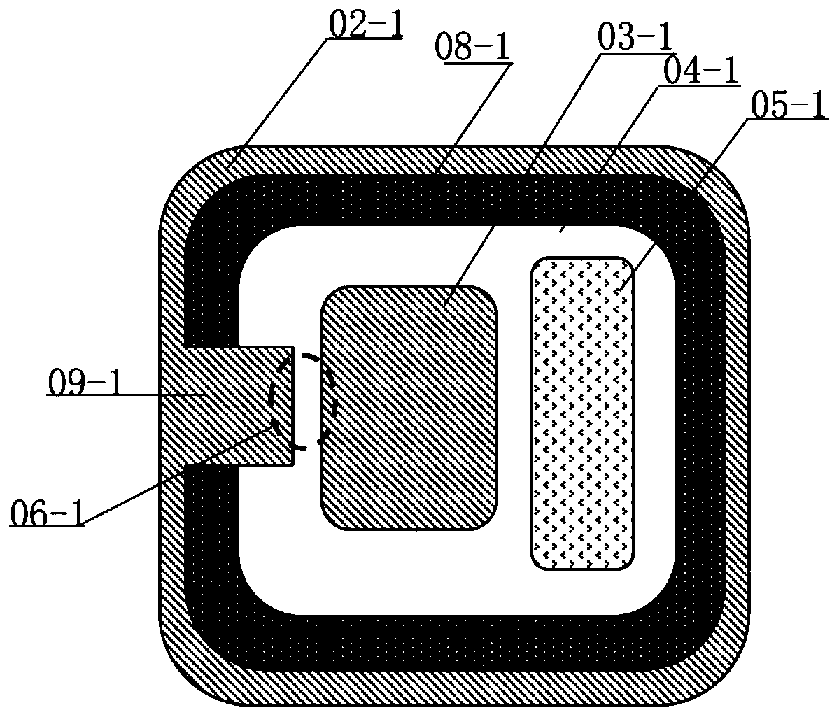
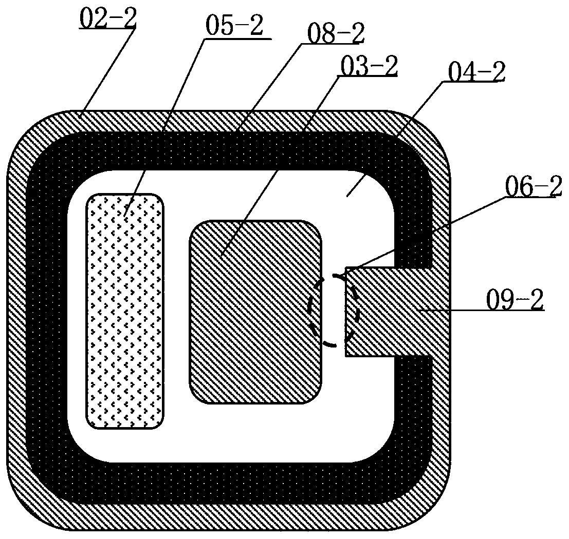
[0051] Such as Figure 4 and Figure 5 as shown, Figure 4 The bidirectional thyristor in the prior art and the figure 1 The structure in is similar, so it will not be repeated here. In this embodiment, only the parts different from those in the prior art will be described in detail. In this embodiment, the substrate is N-type for detailed description. The second N well 03-1 Used to receive trigger pulses and emit carriers to the first N well 02-1, the first N well 02-1 is used to emit carriers to the above N substrate, by increasing the size of the first N well 02 The trigger area 09-1 of -1 solves the technical problem of the small space for electrons in the prior art, and the trigger area of the second N well 03-1 remains unchanged. In the embodiment of the present invention, the first N well 02-1 The trigger area 09-1 of the first N well 02-1 is set to emit design and then the trigger area 09-1 of the first N well 02-1 is set, and the trigger area of the first N wel...
Embodiment 2
[0056] Such as Figure 6 as shown in Figure 4 and Figure 6 As shown, the bidirectional thyristor in this embodiment is different from that in the prior art figure 1 In this embodiment, only the parts different from those in the prior art will be described in detail. When the substrate is an N substrate, this embodiment simultaneously enlarges the first N well 02- The trigger area 09-1 of 1 and the trigger area of the second N well 03-1 are reduced to solve the technical problem in the prior art that the space for electron detachment is small. exist Figure 6 The cross-section of the second N well 02-1 is a quadrangle, or other shapes, but is not limited thereto. A notch-shaped structure is provided on the side of the quadrilateral. The notch-shaped structure can be a groove or other shapes, but is not limited thereto. In this embodiment, the notch-shaped structure is an inverted trapezoidal structure, which is similar to the above-mentioned inverted trapezoidal structu...
Embodiment 3
[0061] Such as Figure 7 as shown in Figure 4 and Figure 7 As shown, the bidirectional thyristor in this embodiment is different from that in the prior art figure 1In this embodiment, only the parts different from those in the prior art are introduced in detail. When the substrate is an N substrate, the trigger region of this embodiment is set in the second N well In order to increase the symmetry of triggering, the triggering area is set at two corner positions of the quadrilateral, which correspond to the corner positions of the first N-well, which can increase the The trigger area can solve the technical problem of the small space for electronic dismissal in the prior art.
[0062] exist Figure 7 The cross-section of the second N well in the middle is a quadrangle, and may also be other shapes, but is not limited thereto. A notch-shaped structure is provided at the corner of the quadrangle, the trigger region 03-11 on the second N well 03-1 is set corresponding to t...
PUM
 Abstract
Description
Claims
Application Information


