Artificial feeling neural circuit and preparation method thereof
A circuit and neural technology, applied in the field of bionic electronics, can solve problems such as complex circuit structure
- Summary
- Abstract
- Description
- Claims
- Application Information
AI Technical Summary
Problems solved by technology
Method used
Image
Examples
Embodiment 1
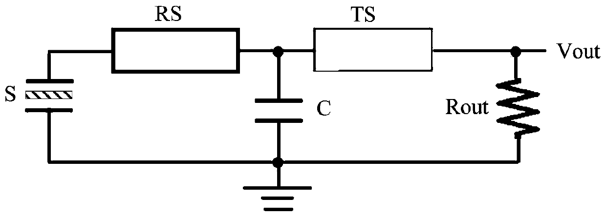
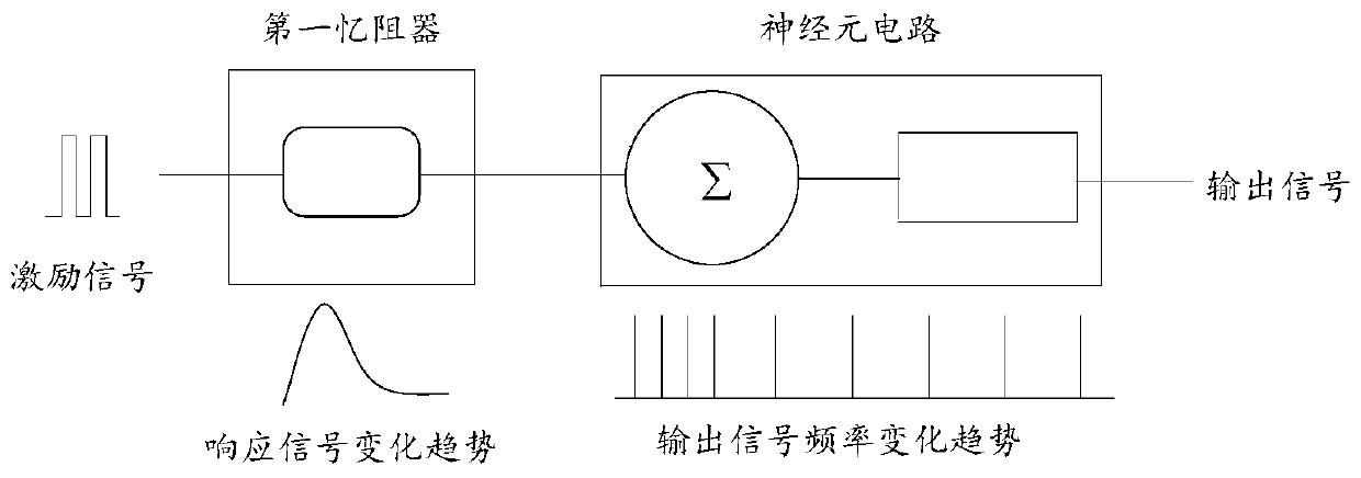
[0055] This embodiment provides an artificial sensory neural circuit, figure 1 is a schematic diagram of the circuit structure of the artificial sensory nerve circuit, and the artificial sensory nerve circuit includes a sensor S, a first memristor RS and a neuron circuit.
[0056] Specifically, the sensor S is used for sensing external signals and generating an excitation signal according to the external signals. The sensor S can be a photoelectric sensor, a pressure sensor, etc., and the type of the sensor S can be determined according to actual application scenarios. The first memristor RS is used to generate a response signal according to the excitation signal. In this embodiment, the first memristor RS has a unidirectional resistance-switching characteristic. The unidirectional resistive switching characteristic is also called unipolar resistive switching behavior, which means that the resistive switching behavior does not depend on the polarity of the applied voltage. A...
Embodiment 2
[0062] Based on the same inventive concept, this embodiment provides a method for preparing an artificial sensory neural circuit. Figure 4 It is a flowchart of the preparation method of the artificial sensory nerve circuit, and the preparation method of the artificial sensory nerve circuit includes step S1 to step S3.
[0063] S1, prepare a neuron circuit, and the neuron circuit is used to charge and discharge according to the response signal to output a pulse signal.
[0064] Figure 5 It is a flowchart of the preparation method of the neuron circuit, and the preparation method of the neuron circuit includes step S11 to step S13.
[0065] S11, preparing the output resistance.
[0066] Such as Figure 6a As shown, a semiconductor substrate 11 is provided, and the semiconductor substrate 11 may be a silicon substrate, a quartz substrate, or an organic flexible film substrate or the like.
[0067] Such as Figure 6b As shown, a first isolation layer 12 is deposited on the ...
PUM
 Abstract
Description
Claims
Application Information


