Flat panel detector

A flat-panel detector and substrate technology, applied in semiconductor devices, electric solid-state devices, radiation control devices, etc., can solve problems such as abnormal image electrical signals

Active Publication Date: 2020-01-07
BOE TECH GRP CO LTD +1
View PDF4 Cites 6 Cited by
  • Summary
  • Abstract
  • Description
  • Claims
  • Application Information

AI Technical Summary

Problems solved by technology

[0004] The embodiment of the present invention provides a flat panel detector, which is used to solve the problem that the electrical signal of the acquired image is abnormal due to the external static electricity of the amorphous silicon X-ray flat panel detector

Method used


Image

  • Flat panel detector
  • Flat panel detector
  • Flat panel detector

Examples


preparation example Construction

[0073] Embodiments of the present invention also provide a method for preparing a flat panel detector, such as Figure 9 shown, including:

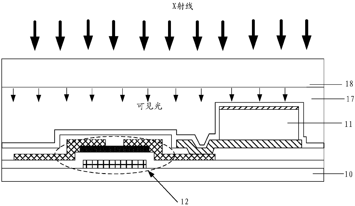
[0074] S10 , forming a photodiode 11 on the substrate 10 .

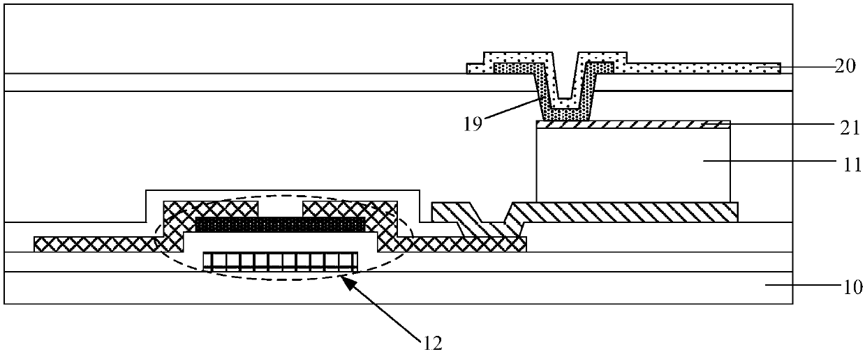
[0075] S20, forming a transmissive conductive layer 20 and a signal line 19 connected to the photodiode 11 on the substrate 10 formed with the photodiode 11, wherein the orthographic projection of the transmissive conductive layer 20 on the substrate 10 is the same as that of the photodiode 11 on the substrate Orthographic overlap on 10.

[0076] In some embodiments, step S20 includes:

[0077] S201 , forming a signal line 19 connected to the photodiode 11 on the substrate 10 formed with the photodiode 11 .

[0078] S202 , forming a transmissive conductive layer 20 on the substrate 10 formed with the signal line 19 .

[0079] That is to say, after the photodiode 11 is formed, the signal line 19 is formed first, and then the transmissive conductive layer 20 is formed.

[008...

Embodiment 1

[0086] prepared as Figure 5 Flat panel detectors shown, including:

[0087] S100 , forming a thin film transistor 12 on a substrate 10 .

[0088] Exemplarily, step S100 includes:

[0089] S110 , forming a gate on the substrate 10 .

[0090] S120, forming a gate insulating layer on the substrate 10 on which the gate is formed.

[0091] S120, forming an active layer on the substrate 10 formed with the gate insulating layer.

[0092] S120, forming a source electrode and a drain electrode on the substrate 10 on which the active layer is formed.

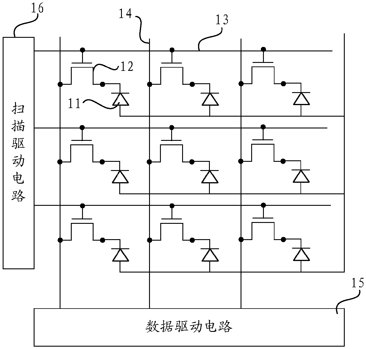
[0093] S200 , forming a photodiode 11 on the substrate 10 on which the thin film transistor 12 is formed.

[0094] Exemplarily, step S200 includes:

[0095] S210 , forming an N-type semiconductor layer on the substrate 10 on which the thin film transistor 12 is formed.

[0096] S220, forming an intrinsic semiconductor layer on the substrate 10 formed with the N-type semiconductor layer.

[0097] S230, forming a P-type semiconduct...

Embodiment 2

[0104] prepared as Figure 6 Flat panel detectors shown, including:

[0105] S100 , forming a thin film transistor 12 on a substrate 10 .

[0106] S200 , forming a photodiode 11 on the substrate 10 on which the thin film transistor 12 is formed.

[0107] S300 , forming a flat layer 17 on the substrate 10 on which the photodiode 11 is formed.

[0108] S400 , forming a signal line 19 on the substrate 10 formed with the planar layer 17 .

[0109] S500 , forming a transmissive conductive layer 20 on the substrate 10 formed with the signal line 19 , the orthographic projection of the transmissive conductive layer 20 on the substrate 10 covers the orthographic projection of the photodiode 11 on the substrate 10 .

[0110] Or S500', synchronously forming a transmissive conductive layer 20 and a conductive pattern on the substrate 10 formed with the signal line 19, the orthographic projection of the transmissive conductive layer 20 on the substrate 10 covers the orthographic projec...


PUM


Abstract

The invention provides a flat panel detector and belongs to the field of flat panel detectors. The invention aims to solve the problem that acquired image electric signals are abnormal due to the influence of the external static electricity of an amorphous silicon X-ray flat panel detector. The flat panel detector comprises a substrate, a plurality of photodiodes arranged on the substrate, and signal lines which are arranged on one sides, far away from the substrate, of the photodiodes and are connected with the photodiodes; the flat panel detector further comprises transmission conducting layers arranged on one sides, away from the substrate, of the photodiodes; and the orthographic projections of the transmission conducting layers on the substrate are overlapped with the orthographic projections of the photodiodes on the substrate.

Description

technical field [0001] The invention relates to the field of flat panel detectors, in particular to a flat panel detector. Background technique [0002] Amorphous silicon (a-Si) X-ray flat panel detector is an X-ray image detector with an amorphous silicon photodiode array as the core. It is converted into visible light, and then transformed into an image electrical signal by an amorphous silicon array with the function of a photodiode, which is transmitted through peripheral circuits and converted from analog to digital to obtain a digital image. Because it has gone through the imaging process of X-ray-visible light-charge image-digital image, it is usually called an indirect conversion flat panel detector. Amorphous silicon X-ray flat panel detectors have the advantages of fast imaging speed, good spatial and density resolution, high signal-to-noise ratio, and direct digital output, so they are widely used in various digital X-ray imaging devices. [0003] Since the amor...

Claims


Application Information

Patent Timeline
Patent Type & Authority Applications(China)
IPC IPC(8): H01L27/146
CPCH01L27/14663H01L27/1462H01L27/14636H01L27/14609H01L27/14692H01L27/14658H01L27/14685
Inventor 张勇华刚薛艳娜林坚包智颖米磊白璐方浩博王景棚张丽敏
Owner BOE TECH GRP CO LTD
Why Eureka
Try Eureka