Single-photon Si-APD detector and manufacturing method thereof

A detector, single-photon technology, used in final product manufacturing, sustainable manufacturing/processing, semiconductor devices, etc., can solve the problems of narrow avalanche zone width, large dark count, damage to silicon lattice, etc., and achieve low electric field intensity. , the structure is novel, the effect of improving the detection efficiency

Active Publication Date: 2020-01-10
THE 44TH INST OF CHINA ELECTRONICS TECH GROUP CORP
View PDF8 Cites 3 Cited by
  • Summary
  • Abstract
  • Description
  • Claims
  • Application Information

AI Technical Summary

Problems solved by technology

The width of the avalanche region prepared by the diffusion method is very narrow, and to achieve a high avalanche probability when the device is working requires a higher electric field strength in the avalanche region, such as Figure 5 As shown, while higher electric field strength will lead to band-to-band tunneling and defect-assisted tunneling, making the dark count larger
The width of the avalanche region prepared by the high-energy implantation method is wider, and the electric field intensity in the avalanche region is lower, such as Image 6 However, the bombardment of high-energy impurity ions in high-energy implantation will damage the silicon lattice and cause defects, which will also increase the dark count

Method used


Image

  • Single-photon Si-APD detector and manufacturing method thereof
  • Single-photon Si-APD detector and manufacturing method thereof
  • Single-photon Si-APD detector and manufacturing method thereof

Examples


Embodiment Construction

[0035] The following will clearly and completely describe the technical solutions in the embodiments of the present invention with reference to the accompanying drawings in the embodiments of the present invention. Obviously, the described embodiments are only some, not all, embodiments of the present invention. Based on the embodiments of the present invention, all other embodiments obtained by persons of ordinary skill in the art without making creative efforts belong to the protection scope of the present invention.

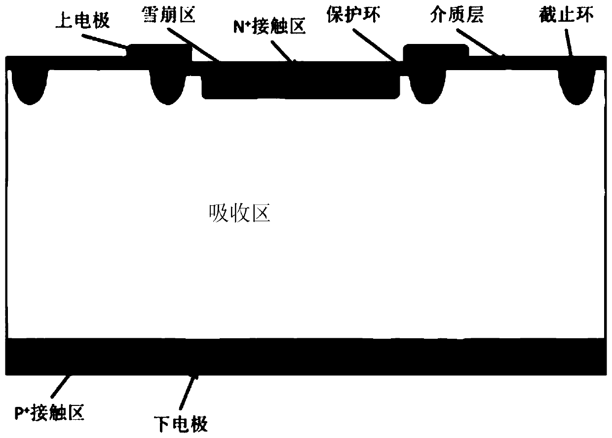
[0036] Such as figure 1 As shown, a single photon Si-APD detector, including: P-type substrate, absorption region, P + Contact area, N + A contact area, an avalanche area, and a dielectric layer, an absorption area is set in the middle of the surface of the P-type substrate, and a P + contact area, the P + A lower electrode is arranged below the contact region; stop rings are arranged at both ends of the upper part of the absorption region; an avalanche re...


PUM


Abstract

The invention provides a single-photon Si-APD detector, which comprises an absorption region, a P+ contact region, an N+ contact region, an avalanche region and a dielectric layer. The absorption region is arranged in the middle of the surface of a P-type substrate; the P+ contact region is arranged under the absorption region; and a lower electrode is arranged under the P+ contact region. Cut-offrings are arranged at the two ends of the upper portion of the absorption region. The avalanche region is arranged in the middle of the upper portion of the absorption region and is formed through compensation doping of P-type impurities and N-type impurities. The N+ contact region is arranged on the avalanche region. The two sides of the avalanche region are each provided with a protection ring,and an upper electrode is arranged above the protection ring. The dielectric layer is arranged on the N+ contact region. The single-photon Si-APD detector has the relatively wide avalanche region andintroduces few defects in the manufacturing process, and can realize device performance of high detection efficiency and low dark counting.

Description

technical field [0001] The invention relates to the field of photodetector chips, in particular to a single-photon Si-APD detector and a manufacturing method thereof. Background technique [0002] Single-photon detection, as a detection technology for extremely weak optical signals, has broad application prospects in the fields of quantum communication, astronomical photometry, medical imaging, and radar detection. In view of its huge scientific research value and strategic position, single-photon detection has become the current One of the hot spots in the field of photoelectric detection. As the core component of the detection system, the single-photon detector determines the performance parameters of the entire single-photon detection system. Therefore, designing a single-photon detector with high detection efficiency and low dark count is one of the key problems that need to be solved urgently. [0003] The single-photon silicon avalanche diode Si-APD is a special photo...

Claims


Application Information

Patent Timeline
Patent Type & Authority Applications(China)
IPC IPC(8): H01L31/0352H01L31/107H01L31/18
CPCH01L31/03529H01L31/107H01L31/1804Y02P70/50
Inventor 郭安然雷仁方李睿智高建威向华兵
Owner THE 44TH INST OF CHINA ELECTRONICS TECH GROUP CORP
Why Eureka
Try Eureka