Three-dimensional stacked phase change memory and preparation method thereof

A technology of phase-change memory and three-dimensional stacking, which is applied in semiconductor devices, electric solid-state devices, electrical components, etc., can solve the problems of reducing unit phase-change operation current, complex multi-layer stacking steps, and difficult process realization, etc., reaching the surface The effect of small unevenness, low power consumption, and small unevenness

A technology of phase-change memory and three-dimensional stacking, which is applied in semiconductor devices, electric solid-state devices, electrical components, etc., can solve the problems of reducing unit phase-change operation current, complex multi-layer stacking steps, and difficult process realization, etc., reaching the surface The effect of small unevenness, low power consumption, and small unevenness

CN110707209AActive Publication Date: 2020-01-17HUAZHONG UNIV OF SCI & TECH

Image

  • Three-dimensional stacked phase change memory and preparation method thereof
  • Three-dimensional stacked phase change memory and preparation method thereof
  • Three-dimensional stacked phase change memory and preparation method thereof

Examples


preparation example Construction

[0042] Such as Figure 1 to Figure 6 As shown, the present invention provides a method for preparing a three-dimensional stacked phase change memory, which specifically includes the following steps:

[0043] (1) A whole layer of electrode material is used as the first horizontal electrode on the substrate;

[0044] (2) Prepare a first insulating layer slightly smaller than the first horizontal electrode in a certain direction (such as the length direction or width direction of the square substrate) on the entire layer of the first horizontal electrode;

[0045] (3) preparing a second horizontal electrode of the same size on the first insulating layer;

[0046] (4) On the above structure, prepare an insulating layer slightly smaller than the second electrode in a certain direction, for example, prepare a second insulating layer smaller than the second horizontal electrode in the same direction as the first insulating layer;

[0047] (5) If more layers are to be stacked, repeat...

Embodiment 1

[0055] This embodiment comprises the following steps:

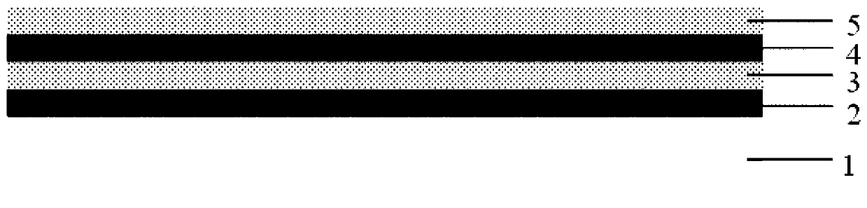
[0056] Step 1: On the single crystal silicon substrate 1 with SiO2 insulating layer on the surface, deposit 100nm Al as the first layer electrode 2 by electron beam evaporation process.

[0057] Step 2: On the basis of Step 1, use PECVD to deposit 100nm SiO 2 It serves as the first insulating layer 3 and exposes the electrode pins of the first layer.

[0058]Step 3: On the basis of Step 2, electron beam evaporation is used to deposit 100nm Al as the second layer of electrode 4, completely located on the first layer of insulating layer.

[0059] Step 4: PECVD growth of 100nm SiO on the basis of Step 3 2 As the second insulating layer 5 and expose the second layer of electrode pins (such as figure 1 shown; figure 1 The exposed pins are not shown in , for details, please refer to Figure 7 ).

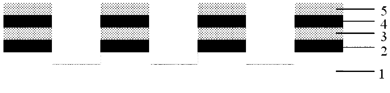
[0060] Step 5: Repeat the above steps for more layers of stacking.

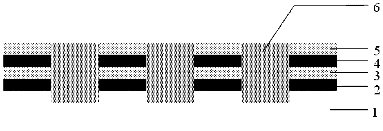
[0061] Step 6: Use ICP etching equipment to regularly ...


PUM


Abstract

The invention belongs to the technical field of microelectronic devices and memories, and discloses a three-dimensional stacked phase change memory and a preparation method thereof. The preparation method specifically comprises the following steps of preparing a multi-layer structure on which a horizontal electrode layer and an insulating layer are crossly stacked, on a substrate; then etching toform a groove and a discrete three-dimensional strip-shaped electrode; filling an insulating medium in the groove, forming small holes in the boundary area of the three-dimensional strip-shaped electrode and the insulating medium, sequentially depositing a phase change material on the walls of the small holes, and filling an electrode material in the small holes to prepare a vertical electrode, thereby obtaining the multi-layer stacked three-dimensional stacked phase change memory. According to the present invention, by improving the whole flow process of the preparation method, a three-dimensional phase change memory array can be established by utilizing the vertical electrode structure, and compared with the prior art, the problems of complex multi-layer stacking steps, high process implementation difficulty, unit size miniaturization and the like of an existing three-dimensional stacked phase change memory in process preparation, can be effectively solved.

Description

technical field [0001] The invention belongs to the technical field of microelectronic devices and memories, and more specifically relates to a three-dimensional stacked phase-change memory and a preparation method thereof. Background technique [0002] The continuous growth of the total amount of data makes the computer put forward higher requirements for the read and write speed, total capacity, energy consumption and stability of the memory. The size of the existing DRAM has reached the technological limit of the manufacturing level, and the influence of various microscopic effects will become more and more obvious in the process of size reduction, so the traditional DRAM technology is facing difficulties in many aspects. A new type of memory, nonvolatile memory, offers a new way to expand computer memory. As the mainstream non-volatile memory in the market today, flash memory will not lose the data stored in it even in the event of a sudden power failure. However, the ...

Claims


Application Information

Patent Timeline
17 Jan 2020
Publication
CN110707209A
IPC
H01L45/00; H01L27/24
CPC
H10B63/845; H10B63/84; H10N70/841; H10N70/011; H10N70/823; H10N70/231; H10N70/8825; H10N70/023
Inventors
童浩; 蔡旺