A positioning device for semiconductor device welding

A positioning device and semiconductor technology, applied in auxiliary devices, welding equipment, auxiliary welding equipment, etc., can solve the problems of inability to meet modern production, low safety factor of manual operation, etc., to save labor costs, high safety factor, and ensure processing accuracy. Effect

Active Publication Date: 2021-04-27
WENZHOU UNIV
View PDF6 Cites 0 Cited by
  • Summary
  • Abstract
  • Description
  • Claims
  • Application Information

AI Technical Summary

Problems solved by technology

[0002] A semiconductor device is an electronic device whose conductivity is between a good conductor and an insulator. It uses the special electrical characteristics of semiconductor materials to complete specific functions. It can be used to generate, control, receive, transform, amplify signals and perform energy conversion. The semiconductor of semiconductor devices The material is silicon, germanium or gallium arsenide, which can be used as rectifiers, oscillators, light emitters, amplifiers, photometers and other equipment. In order to distinguish them from integrated circuits, they are sometimes called discrete devices. Most of the two-terminal devices The basic structure is a PN junction. When processing semiconductor devices, manual loading and unloading and positioning operations are required, which cannot meet the requirements of modern production, and the safety factor of manual operation is low.

Method used


Image

  • A positioning device for semiconductor device welding
  • A positioning device for semiconductor device welding
  • A positioning device for semiconductor device welding

Examples


Embodiment

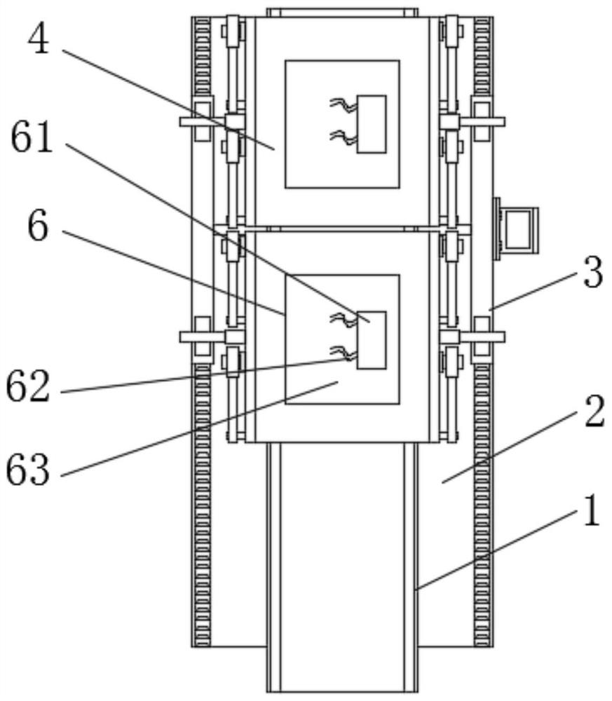
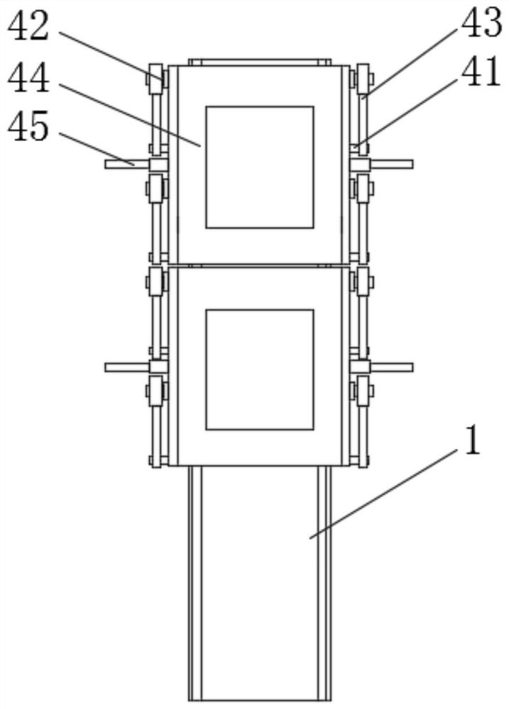
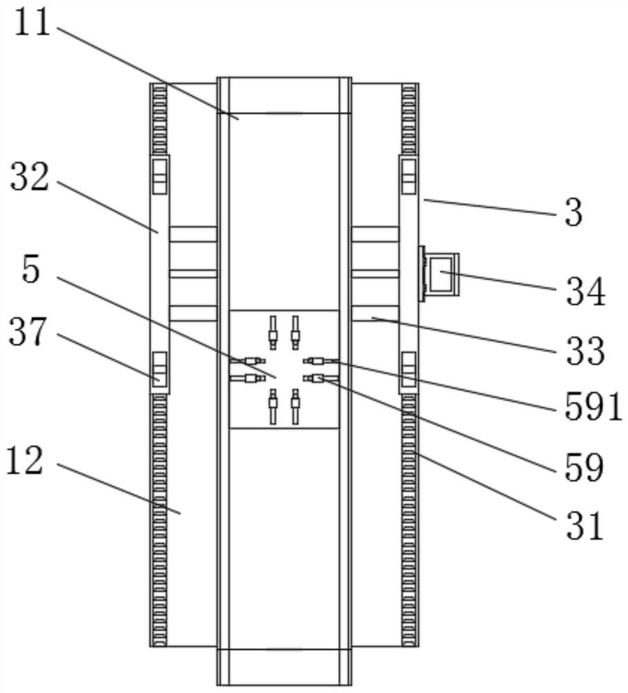
[0024] Example: such as Figure 1-7 As shown, a positioning device for semiconductor device welding of the present invention includes a material platform 1, an extension plate 2, a translation mechanism 3, a loading and unloading mechanism 4, a limit mechanism 5 and an adsorption mechanism 6, and the outer side of the material platform 1 is provided with a through groove 11. Both sides of the material platform 1 are fixedly connected with extension plates 2, the middle part of the material platform 1 is provided with a limit mechanism 5, and the translation mechanism 3 includes a rail rack 31, a guard plate 32, a connecting plate 33, a No. 1 servo motor 34, The driving rod 35, the driving gear 36 and the shift fork 37, the track rack 31 are fixedly connected to the upper side of the extension plate 2, the upper side of the track rack 31 is provided with a guard plate 32, and a connecting plate 32 is provided between the two guard plates 32. Plate 33 and drive rod 35, connectin...


PUM


Abstract

The invention discloses a positioning device for semiconductor device welding, which comprises a material platform, an extension plate, a translation mechanism, a loading and unloading mechanism, a limit mechanism and an adsorption mechanism. The outer side of the material platform is provided with a through groove, and both sides of the material platform are fixed. There is an extension plate connected, and a limit mechanism is set in the middle of the material table. The translation mechanism includes a track rack, a guard plate, a connecting plate, a No. 1 servo motor, a drive rod, a drive gear and a shift fork. The track rack is fixedly connected to the extension plate. On the upper side, the upper side of the track rack is equipped with a guard plate, and a connecting plate and a driving rod are arranged between the two guard plates. The connecting plate and the guard plate are fixedly connected. The present invention has compact structure, reasonable structural design and high degree of automation. In specific use, the translation mechanism can move the horizontal cover plate in the loading and unloading mechanism to reciprocate. The loading and unloading mechanism cooperates with the adsorption mechanism to realize the handling process of semiconductor devices. The limit mechanism can accurately move semiconductor devices from four directions. position.

Description

technical field [0001] The invention relates to a positioning device, in particular to a positioning device for semiconductor device welding, which belongs to the technical field of semiconductor device processing. Background technique [0002] A semiconductor device is an electronic device whose conductivity is between a good conductor and an insulator. It uses the special electrical characteristics of semiconductor materials to complete specific functions. It can be used to generate, control, receive, transform, amplify signals and perform energy conversion. The semiconductor of semiconductor devices The material is silicon, germanium or gallium arsenide, which can be used as rectifiers, oscillators, light emitters, amplifiers, photometers and other equipment. In order to distinguish them from integrated circuits, they are sometimes called discrete devices. Most of the two-terminal devices The basic structure is a PN junction. During the processing of semiconductor devices...

Claims


Application Information

Patent Timeline
Patent Type & Authority Patents(China)
IPC IPC(8): B23K37/04B23K37/00
CPCB23K37/00B23K37/0435
Inventor 施一剑陈博金才垄李刚
Owner WENZHOU UNIV
Why Eureka
Try Eureka