Micro three-dimensional stacked MEMS (Micro Electro Mechanical System) resonance device

A resonant, three-dimensional technology, which is applied in the field of micro-three-dimensional stacked MEMS resonant devices, can solve the problems that the heating phenomenon of the application-specific integrated circuit cannot be completely eliminated, the strength of the shell structure cannot be increased without limit, and the deformation of the chip structure cannot be avoided, etc., to achieve convenient electrical Effects of connection, guaranteed performance, and reduced process complexity

Active Publication Date: 2020-02-11
CHINA ELECTRONICS TECH GRP NO 26 RES INST
View PDF16 Cites 1 Cited by
  • Summary
  • Abstract
  • Description
  • Claims
  • Application Information

AI Technical Summary

Problems solved by technology

However, these methods have disadvantages: one is that it is impossible to choose a material with the same thermal expansion coefficient as the resonant chip material to make the shell; The structure of the chip is deformed; the third is that due to the limitation of volume, material and process, the structural strength of the shell cannot be increased without limit; the fourth is to further miniaturize the resonant chip and the application-specific integrated circuit, which often requires the system optimization of the overall structure and performance of the product , It is difficult and difficult to realize, and the heating phenomenon cannot be completely eliminated when the ASIC is working.
The above method cannot fundamentally solve the impact of packaging on the stability of MEMS resonant devices, and cannot effectively solve the problem of miniaturization

Method used


Image

  • Micro three-dimensional stacked MEMS (Micro Electro Mechanical System) resonance device
  • Micro three-dimensional stacked MEMS (Micro Electro Mechanical System) resonance device
  • Micro three-dimensional stacked MEMS (Micro Electro Mechanical System) resonance device

Examples


Embodiment Construction

[0023] The present invention will be further described in detail below in conjunction with the accompanying drawings.

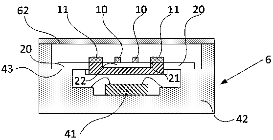
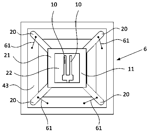
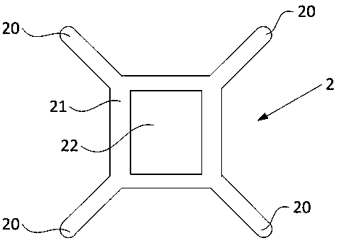
[0024] Such as figure 1 and figure 2 As shown, the present invention discloses a miniature three-dimensional stacked MEMS resonator device, comprising an open shell 42 and a cap 62 with an open airtight shell 42, and also includes a conductive chip support 2, the chip support 2 and the resonator Chip 1 has the same thermal expansion coefficient (chip holder 2 and resonant chip 1 can be made of the same material), resonant chip 1 includes a resonant beam 10 and a fixed part 11, and resonant chip 1 is mounted on the chip holder 2 through the fixed part 11 and makes the resonant beam 10 is suspended in the air, the chip support 2 is installed on the inner wall of the shell 42 and is electrically connected with the shell 42, the inner bottom surface of the shell 42 below the chip support 2 is provided with an integrated chip 41 mounting groove, and the integra...


PUM


Abstract

The invention discloses a micro three-dimensional stacked MEMS (Micro Electro Mechanical System) resonance device. The device comprises a shell and a cap sealing an opening of the shell. The device also comprises a conductive chip support. The chip support and the resonance chip have the same thermal expansion coefficient; the resonance chip comprises a resonance beam and a fixing part, wherein the resonance chip is installed on the chip support through the fixing part, the resonance beam is suspended, the chip support is installed on the inner wall of the shell and electrically connected with the shell, an integrated chip installation groove is formed in the inner bottom surface of the shell below the chip support, and an integrated chip electrically connected with the shell is installedin the integrated chip installation groove. The resonance chip and the shell are connected by the chip support, so that the resonance chip is prevented from being influenced by shell deformation andthermal stress; a resonance chip, a chip support and an integrated chip are installed by adopting a three-dimensional stacked structure, the size of the MEMS resonance device is effectively reduced, and the miniature three-dimensional stacked MEMS resonance device disclosed by the invention can realize miniaturization of the MEMS resonance device on the premise of meeting the stability requirementof the MEMS resonance device.

Description

technical field [0001] The invention relates to the technical field of MEMS resonant devices, in particular to a miniature three-dimensional stacked MEMS resonant device. Background technique [0002] MEMS (Micro-Electro-Mechanical Systems) is the abbreviation of micro-electro-mechanical systems. MEMS chip manufacturing uses microelectronic processing technology, especially three-dimensional micro-body processing technology, to manufacture various micro-mechanical structure-sensitive chips, and then integrates them with application-specific integrated circuits. Constitute miniaturized and intelligent sensors, actuators, optical devices and other MEMS devices and components, such as crystal resonators, angular velocity sensors, acceleration sensors, pressure sensors and temperature sensors. MEMS devices and components have the characteristics of small size, high reliability, strong environmental adaptability, low power consumption, low cost, etc., and are widely used in aeros...

Claims


Application Information

Patent Timeline
IPC IPC(8): B81B7/02B81B7/00
CPCB81B7/0032B81B7/02B81B2201/0271
Inventor 林日乐谢佳维王伟李文蕴蒋昭兴罗华
Owner CHINA ELECTRONICS TECH GRP NO 26 RES INST
Why Eureka
Try Eureka