A mesa-type photodiode with graded barrier and low dark current and its manufacturing method

A photodiode, mesa-type technology, applied in circuits, electrical components, semiconductor devices, etc., can solve problems such as surface leakage current and bulk dark current that cannot be reduced

Active Publication Date: 2021-07-06
THE 44TH INST OF CHINA ELECTRONICS TECH GROUP CORP
View PDF4 Cites 0 Cited by
  • Summary
  • Abstract
  • Description
  • Claims
  • Application Information

AI Technical Summary

Problems solved by technology

[0004] However, the surface leakage current and bulk dark current cannot be reduced in this structure, so there is an urgent need for a mesa photodiode that can reduce the surface leakage current and bulk dark current.

Method used


Image

  • A mesa-type photodiode with graded barrier and low dark current and its manufacturing method
  • A mesa-type photodiode with graded barrier and low dark current and its manufacturing method
  • A mesa-type photodiode with graded barrier and low dark current and its manufacturing method

Examples


Embodiment Construction

[0031] The following will clearly and completely describe the technical solutions in the embodiments of the present invention with reference to the accompanying drawings in the embodiments of the present invention. Obviously, the described embodiments are only some, not all, embodiments of the present invention. Based on the embodiments of the present invention, all other embodiments obtained by persons of ordinary skill in the art without making creative efforts belong to the protection scope of the present invention.

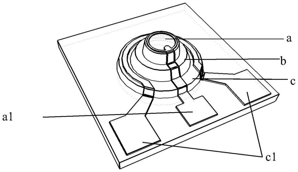
[0032] The invention is a mesa-type photodiode with low dark current of graded potential barrier, such as figure 1 As shown, it includes a three-layer mesa structure, N-type mesa a, absorption mesa b, and P-type mesa c connected sequentially from top to bottom, and the bottom layer of the P-type mesa step is a semi-insulating substrate 1 .

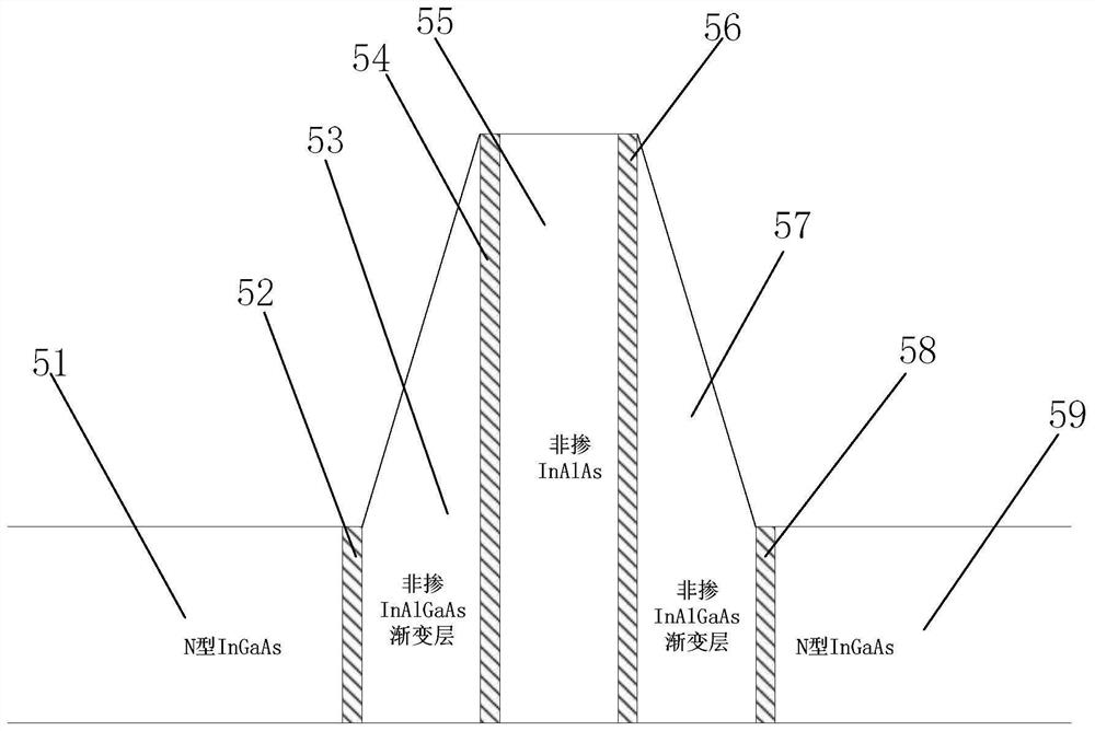
[0033] Such as figure 2 As shown, the surface of each mesa of the mesa-type photodiode is covered with a passivation l...


PUM

PropertyMeasurementUnit
thicknessaaaaaaaaaa
thicknessaaaaaaaaaa
thicknessaaaaaaaaaa

Abstract

The invention belongs to the technical field of detector chip manufacture, and relates to a mesa-type photodiode with low dark current in a graded potential barrier; an N-type mesa, an absorption mesa and a P-type mesa connected from top to bottom of the mesa-type photodiode; each mesa The surface of the mesa photodiode is covered with a passivation layer; a graded barrier layer is arranged in the absorption mesa of the mesa photodiode, and the graded barrier layer has a nine-layer structure from top to bottom; an N electrode is arranged on the N-type mesa, and the The P-type mesa is provided with a P electrode, and the P electrode and the N electrode form a coplanar electrode; the present invention reduces the surface leakage current and the bulk dark current of the mesa photodiode by adopting a hierarchical barrier structure, thereby improving the mesa photodiode. reliability.

Description

technical field [0001] The invention belongs to the technical field of detector chip manufacture, and in particular relates to a mesa-type photodiode with a graded potential barrier and low dark current and a manufacturing method thereof. Background technique [0002] With the evolution of photodiodes to high-speed and high-bandwidth, the fabrication process is gradually changing from a planar process to a mesa process. The mesa etching process destroys the periodic integrity of the lattice, exposes the surface of the semiconductor material to the environment, introduces surface interface states, and inevitably increases the surface dark current. The composition of dark current also includes: generation of recombination current, diffusion current, interband tunneling current and auxiliary tunneling current, etc. High dark current reduces the performance and reliability of mesa photodiodes, and there is a greater risk of failure. [0003] There are many preparations of mesa...

Claims


Application Information

Patent Timeline
Patent Type & Authority Patents(China)
IPC IPC(8): H01L31/0352H01L31/105H01L31/0224H01L31/18
CPCH01L31/022408H01L31/03529H01L31/105H01L31/1844
Inventor 黄晓峰张承王立唐艳莫才平迟殿鑫崔大健高新江
Owner THE 44TH INST OF CHINA ELECTRONICS TECH GROUP CORP
Why Eureka
Try Eureka