thin film transistor

A technology of thin film transistors and substrates, applied in the direction of transistors, semiconductor devices, electrical components, etc., can solve the problems of IGZO thin film damage, low quality of thin film transistors, affecting the current switching ratio of IGZO thin film transistors, surface carrier concentration, etc., to achieve Effects of reducing surface leakage current, reducing concentration, and improving current switching ratio

Active Publication Date: 2016-08-24
深圳市金誉半导体股份有限公司
View PDF7 Cites 0 Cited by
  • Summary
  • Abstract
  • Description
  • Claims
  • Application Information

AI Technical Summary

Problems solved by technology

However, because the IGZO film is easily affected by environmental factors such as the temperature of the external environment, oxygen content, water vapor, and light, when the IGZO film is prepared by the sputtering process, the plasma in the process will damage the IGZO film, thereby affecting the IGZO thin film transistor. The current switch ratio, surface carrier concentration and other parameters make the quality of thin film transistors not high

Method used


Image

  • thin film transistor
  • thin film transistor
  • thin film transistor

Examples


Embodiment Construction

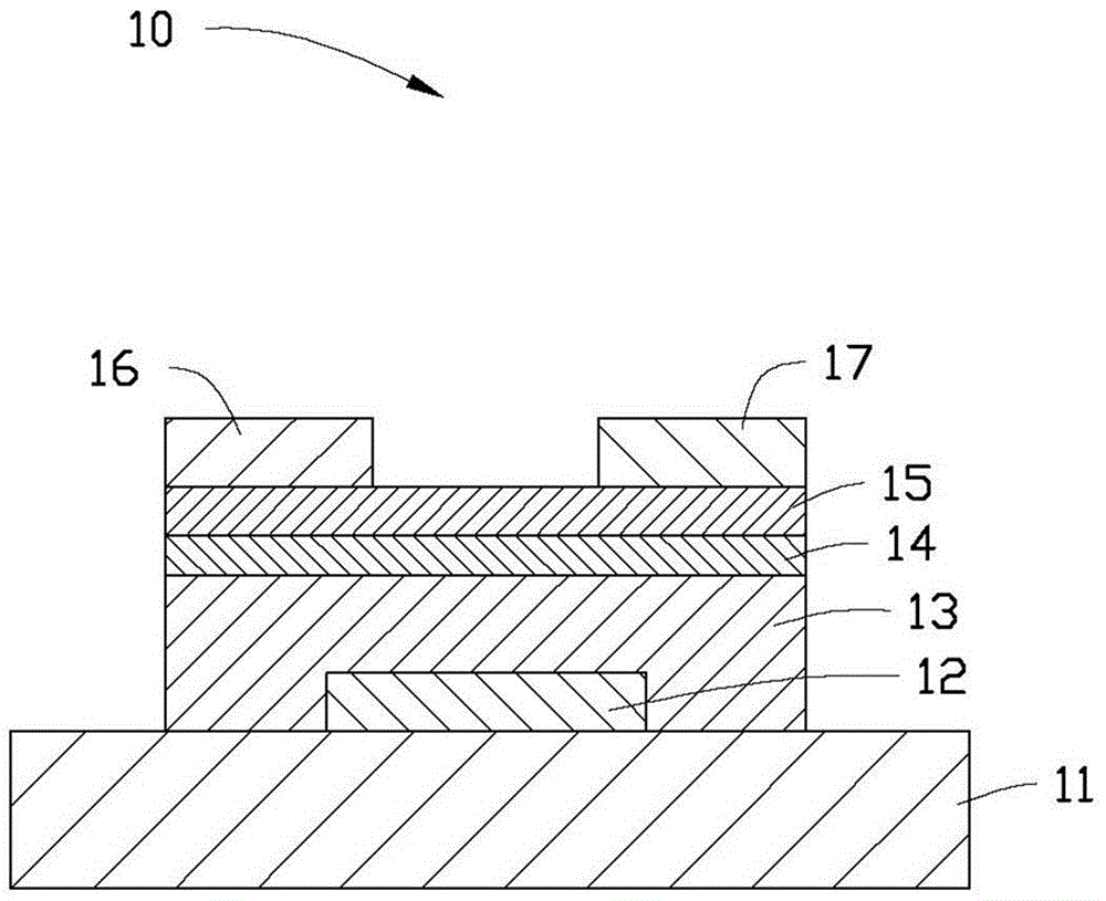
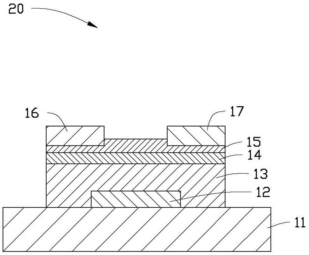
[0014] See figure 1 The thin film transistor 10 provided by the first embodiment of the present invention includes a substrate 11, a gate 12, a gate insulating layer 13, a channel layer 14, a gallium zinc oxide (GaZnO) layer 15, a source 16 and a drain 17.

[0015] The substrate 11 is used to carry the gate electrode 12 and the gate insulating layer 13. The substrate 11 can be made of glass, quartz, silicon wafer, polycarbonate, polymethyl methacrylate, or metal foil.

[0016] The grid 12 is provided on the surface of the substrate 11. In this embodiment, the gate 12 is arranged in the central area of ​​the substrate 11. The grid 12 is made of materials selected from copper, aluminum, nickel, magnesium, chromium, molybdenum, tungsten, and alloys thereof.

[0017] The gate insulating layer 13 covers the surface of the gate 12. In this embodiment, the gate insulating layer 13 extends to contact the substrate 11. The gate insulating layer 13 is made of silicon oxide SiOx, silicon ni...


PUM


Abstract

The invention provides a thin-film transistor comprising a substrate, a grid electrode which is arranged on the substrate, a grid insulating layer which is arranged on the substrate and covers the grid electrode, an indium gallium zinc oxide channel layer which covers the surface of the grid insulating layer, and a gallium oxide zinc layer which is arranged on the surface of the channel layer. A source electrode and a drain electrode are formed on the two opposite sides of the gallium oxide zinc layer. The thin-film transistor with the structure has advantages of being low in surface leakage current and great in current switch ratio.

Description

Technical field [0001] The invention relates to a thin film transistor. Background technique [0002] With the advancement of process technology, thin film transistors have been widely used in displays to meet the needs of thinning and miniaturization of displays. Thin film transistors generally include gate, drain, source, and channel layer components, which change the conductivity of the channel layer by controlling the voltage of the gate, so that the source and drain are turned on or off. status. [0003] Indium Gallium Zinc Oxide (IGZO) thin film transistors have been extensively researched and applied to liquid crystal panels, especially high-resolution and large-size panels. However, because the IGZO film is easily affected by environmental factors such as temperature, oxygen content, water vapor, and light in the external environment, when the IGZO film is prepared by the sputtering process, the plasma in the process will cause damage to the IGZO film, which will affect t...

Claims


Application Information

Patent Timeline
Patent Type & Authority Patents(China)
IPC IPC(8): H01L29/786H01L29/24
CPCH01L29/7869
Inventor 顾南雁杨东霓巴利生胡慧雄
Owner 深圳市金誉半导体股份有限公司
Why Eureka
Try Eureka