Silicon-controlled rectifier and manufacturing method thereof

A technology of silicon controlled rectifiers and manufacturing methods, applied in the direction of electric solid state devices, semiconductor devices, electrical components, etc.

Pending Publication Date: 2020-02-28
SHANGHAI HUALI MICROELECTRONICS CORP
View PDF4 Cites 1 Cited by
  • Summary
  • Abstract
  • Description
  • Claims
  • Application Information

AI Technical Summary

Problems solved by technology

Figure 1C As shown, the leakage performance of the silicon controlled rectifier of the first prior art is about 5nA/30μm, such leak

Method used


Image

  • Silicon-controlled rectifier and manufacturing method thereof
  • Silicon-controlled rectifier and manufacturing method thereof
  • Silicon-controlled rectifier and manufacturing method thereof

Examples


no. 1 example

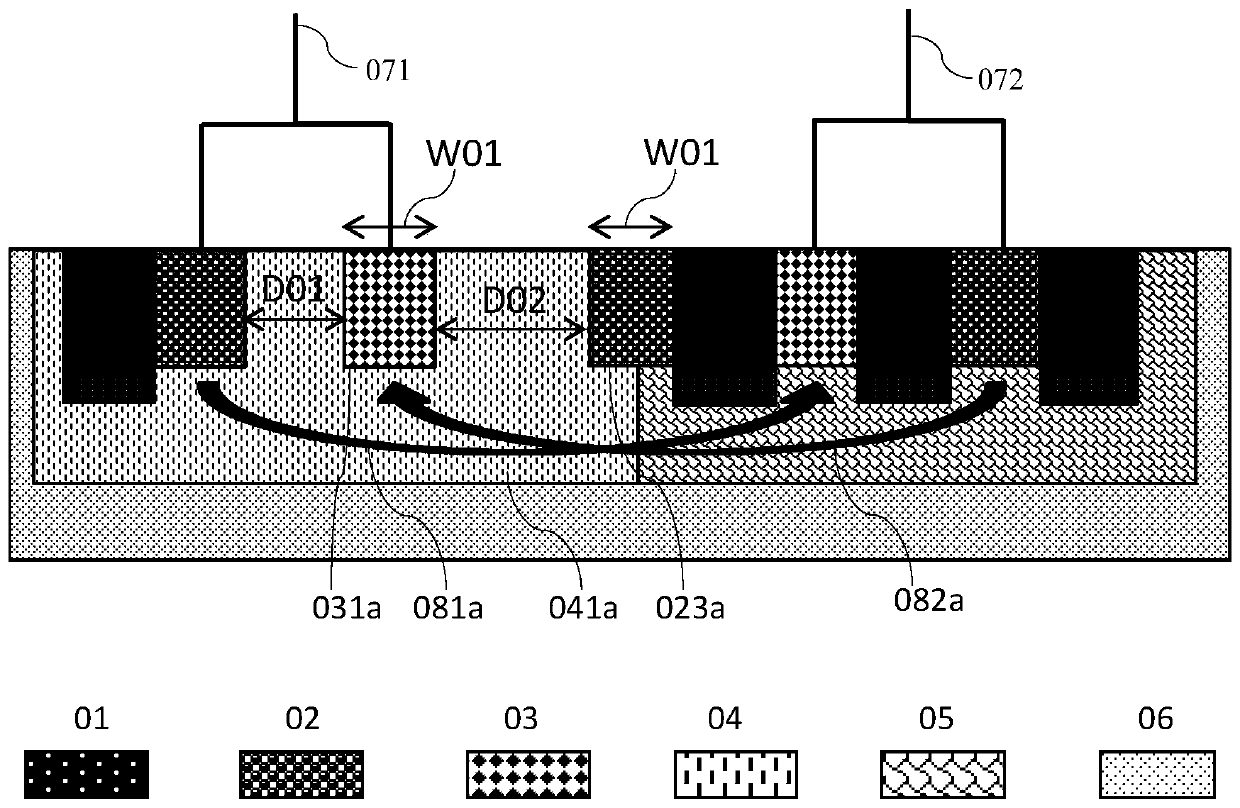
[0125] refer to figure 2 As shown, the first embodiment of the silicon controlled rectifier provided by the present invention: the third high-concentration P-type doping 23 is located in the entire width of the upper part of the P well 51 .

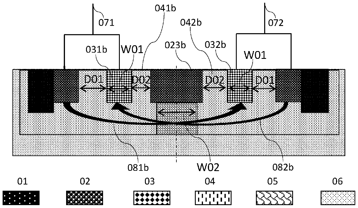
[0126] refer to image 3 As shown, the second embodiment of the silicon controlled rectifier provided by the present invention is different from the first embodiment in that: the third high-concentration P-type doping 23 is located in the entire width of the upper part of the P well 51, the first N well 41 and the first N well 41 The upper part of the junction of the P well 51 and the upper part of the junction of the P well 51 and the second N well 42 . A third high-concentration P-type dopant 23 is formed across the junction of the first N well 41 and the P well 51 , the P well 51 , and the upper part of the junction of the P well 51 and the second N well 42 .

[0127] refer to figure 2 with image 3 As shown, the first device ele...


PUM


Abstract

The invention provides a silicon-controlled rectifier and a manufacturing method thereof. The silicon-controlled rectifier comprises a semiconductor substrate, a first N well, a P well, a second N well, first/second high-concentration P-type doping, first/second high-concentration N-type doping and third high-concentration P-type doping, wherein the first N well, the P well and the second N well are adjacent in sequence; the first/second high-concentration P-type doping and the first/second high-concentration N-type doping are located on the upper part of the first/second N well; the third high-concentration P-type doping is located at the upper part of the P well; a first/second grid electrode is arranged above the first/second N well between the first/second high-concentration N-type doping and the third high-concentration P-type doping; and the first/second high-concentration P-type doping, the first/second high-concentration N-type doping and the first/second grid electrode are connected to form a first/second device pole. Accordingly, the first/second device pole is connected with the input and output end of the positive/negative high voltage, PNPN channels without a conduction condition are formed, a bidirectional anti-static protection function suitable for the positive/negative high voltage at the same time is achieved in an applied circuit, and good electric leakage performance is achieved.

Description

technical field [0001] The invention relates to the technical field of semiconductor integrated circuit devices, in particular to a silicon controlled rectifier. [0002] The invention also relates to the technical field of manufacturing semiconductor devices, in particular to a method for manufacturing a silicon controlled rectifier. Background technique [0003] In the field of high-voltage integrated circuit anti-static protection (ESD, Electro-Static Discharge) design, in the prior art, no hysteresis effect silicon-controlled rectifier (No-Snapback SCR, No-Snapback Silicon ControlledRectifier) ​​multi-stage series connection is applied to the high-voltage port The design scheme of anti-static protection circuit, the technical effect of this technical scheme is that the design has the advantage of saving layout area, so this technical scheme has attracted wide attention. [0004] Prior Art Chinese Patent Application Publication No. CN108183101A discloses a silicon-contro...

Claims


Application Information

Patent Timeline
IPC IPC(8): H01L29/06H01L27/02
CPCH01L29/0603H01L29/0684H01L27/0248
Inventor 朱天志
Owner SHANGHAI HUALI MICROELECTRONICS CORP
Why Eureka
Try Eureka