Supercharge Your Innovation With Domain-Expert AI Agents!

Optical fingerprint recognition circuit

A circuit and circuit processing technology, which is applied in character and pattern recognition, acquisition/organization of fingerprints/palmprints, electrical components, etc., can solve the problem of low fingerprint recognition rate, improve the signal-to-noise ratio of the output signal, and improve the static working point , Improve the effect of fingerprint recognition rate

Pending Publication Date: 2020-03-03
HUAWEI TECH CO LTD
View PDF11 Cites 5 Cited by
  • Summary
  • Abstract
  • Description
  • Claims
  • Application Information

AI Technical Summary

Problems solved by technology

[0005] The application provides an optical signal processing circuit and electronic equipment, which are used to solve the problem of low fingerprint recognition rate existing in the prior art

Method used


Image

  • Optical fingerprint recognition circuit
  • Optical fingerprint recognition circuit
  • Optical fingerprint recognition circuit

Examples


Embodiment Construction

[0045] The technical solution in this application will be described below with reference to the accompanying drawings.

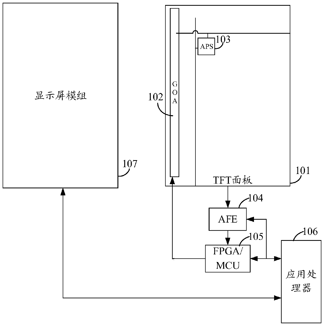
[0046] figure 1 A frame diagram of a fingerprint collection system provided by an embodiment of the present application is shown. The fingerprint collection system of the embodiment of the present application can be used for off-screen fingerprint detection of terminal devices such as mobile phones and tablets. The fingerprint collection system includes a TFT panel 101, a gate driver on array (GOA) 102, an active pixel sensor (active pixel sensor, APS) 103, an analog front end (AFE) 104, and on-site Programmable gate array (field programmable gate array) / microcontroller (microcontroller unit) 105 , application processor (application processor) 106 , display module 107 .

[0047] Among them, the TFT panel 101 is the panel where the fingerprint sensor is located, and its side is the GOA 102, which is used for sequentially gating the row selection lines. The...


PUM


Abstract

The invention provides an optical signal processing circuit and electronic equipment, which can improve the signal-to-noise ratio of an output signal of a fingerprint sensor so as to improve the fingerprint recognition rate. The optical signal processing circuit comprises a photosensitive device, an amplifying tube T1, a switching tube T2, a switching tube T3, a reading circuit, a control circuitand a voltage-adjustable power supply. Due to the fact that when the optical signal processing circuit is in the compensation reset stage, the grid voltage of the T1 just reaches the level enabling the amplifying tube T1 to be turned on, when the input voltage and the voltage increment are applied to the grid of the T1 again, the grid-source voltage Vgs of the T1 is increased, the T1 amplifies aninput voltage signal, and an output signal is generated.

Description

technical field [0001] The present application relates to the field of circuits, and more specifically, to an optical signal processing circuit and an optical fingerprint recognition system. Background technique [0002] Under-screen optical fingerprint recognition is becoming the standard configuration of current mobile phone products. Users can press their fingers on a certain position on the screen to activate the fingerprint recognition function. Specifically, the finger is irradiated with light from the light source under the screen, and the reflected light of the finger carries fingerprint information and is received by the image sensor under the screen to generate a fingerprint image, and then extract fingerprint features, which can be used to realize functions such as unlocking and payment. Thereby improving the security performance of the mobile phone. [0003] In a fingerprint recognition solution in the prior art, a large-area optical fingerprint sensor based on ...

Claims


Application Information

Patent Timeline
IPC IPC(8): G06K9/00H03K17/96
CPCH03K17/9627G06V40/1318
Inventor 王希林张宏海夏丽林
Owner HUAWEI TECH CO LTD
Features
  • R&D
  • Intellectual Property
  • Life Sciences
  • Materials
  • Tech Scout
  • Unparalleled Data Quality
  • Higher Quality Content
  • 60% Fewer Hallucinations
Learn More