High-reliability rectification device application chip with composite inner passive film single-groove structure

A rectifier device and reliability technology, applied in semiconductor devices, electrical components, circuits, etc., can solve problems such as poor reliability and poor high temperature characteristics, and achieve the effect of increasing voltage, good thermal stability, and increasing breakdown voltage

Pending Publication Date: 2020-03-17
安徽微半半导体科技有限公司
View PDF0 Cites 1 Cited by
  • Summary
  • Abstract
  • Description
  • Claims
  • Application Information

AI Technical Summary

Problems solved by technology

[0003] The technical problem to be solved by the present invention lies in the poor reliability and poor high temperature characteristics of the protective film using glass as the passivation layer in the trench

Method used


Image

  • High-reliability rectification device application chip with composite inner passive film single-groove structure

Examples


Embodiment Construction

[0021] The specific implementation will be described in detail below in conjunction with the accompanying drawings:

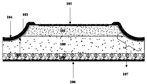
[0022] 109 figure 1 A schematic structural diagram of an embodiment of the present invention is given. In the figure, a compound internal passivation layer structure of a silicon rectifier device includes: a middle layer 100 single crystal semiconductor body, an upper layer 101 is a chip body with a P-type doped layer or an N-type doped layer, and a lower layer 108 is an N-type The chip body of the doped layer or the P-type doped layer (see 108 above for details), the mesa 107, the upper electrode metal layer 105, the lower electrode metal layer 106, the polysilicon thin film in the mesa structure region and the nanoscale high-purity oxidation layer underneath it. Layer 102, silicon nitride film 103 in the mesa structure area, glass passivation layer 104 made of special glass material; the polysilicon film in the mesa structure area and the nanoscale high-puri...


PUM


Abstract

The invention provides a high-reliability rectification device application chip with a composite inner passivation film single-groove structure. A chip mesa adopts a single-groove design, the surfaceof the inner wall of a groove adopts a composite inner passivation layer structure, and a composite inner passivation layer is composed of a polycrystalline silicon film, a bottom layer high-purity nanoscale oxide film, a silicon nitride film and glass. The chip is composed of a single crystal semiconductor body on the middle layer, a chip body with a P-type boron junction region on the upper layer and an N-type phosphorus junction region on the lower layer, a table board, an upper electrode metal layer and a lower electrode metal layer. According to the invention, the problems of poor reliability and poor high-temperature characteristics of a protective film with glass as a passivation layer in a chip groove are solved.

Description

technical field [0001] The invention relates to a semiconductor device, in particular to a compound internal passivation film single groove high reliability rectifier device application chip. Background technique [0002] In the prior art, the semiconductor rectifier device uses a passivation structure on the inner wall surface of the chip groove to protect the P / N junction of the chip from the interference and influence of external water vapor and impurities. At present, simple, single-layer glass is usually used in the industry. layer, as a passivation structure material on the surface of the groove inner wall of the semiconductor rectifier device application chip, although its process is simple and the cost is low, the thermal expansion coefficient of the glass is poorly matched with the silicon substrate, and the glass is easily broken during use or chip operation. The ability to fix and prevent harmful impurities is not good, such as the ability of sodium ions to contam...

Claims


Application Information

Patent Timeline
Patent Type & Authority Applications(China)
IPC IPC(8): H01L29/06H01L29/12
CPCH01L29/0611H01L29/12
Inventor 冯亚宁曹孙根黄志祥朱浩然汪海波
Owner 安徽微半半导体科技有限公司
Why Eureka
Try Eureka