Multi-level boosted circuit and device and system thereof
A step-up circuit and multi-level technology, applied in control/regulation systems, output power conversion devices, electrical components, etc., can solve the problems of easy control of the bus voltage and easy breakdown of the lower arm switch tube, etc., to achieve The effect of reducing the probability of electric shock accidents
- Summary
- Abstract
- Description
- Claims
- Application Information
AI Technical Summary
Problems solved by technology
Method used
Image

Examples
Embodiment 1
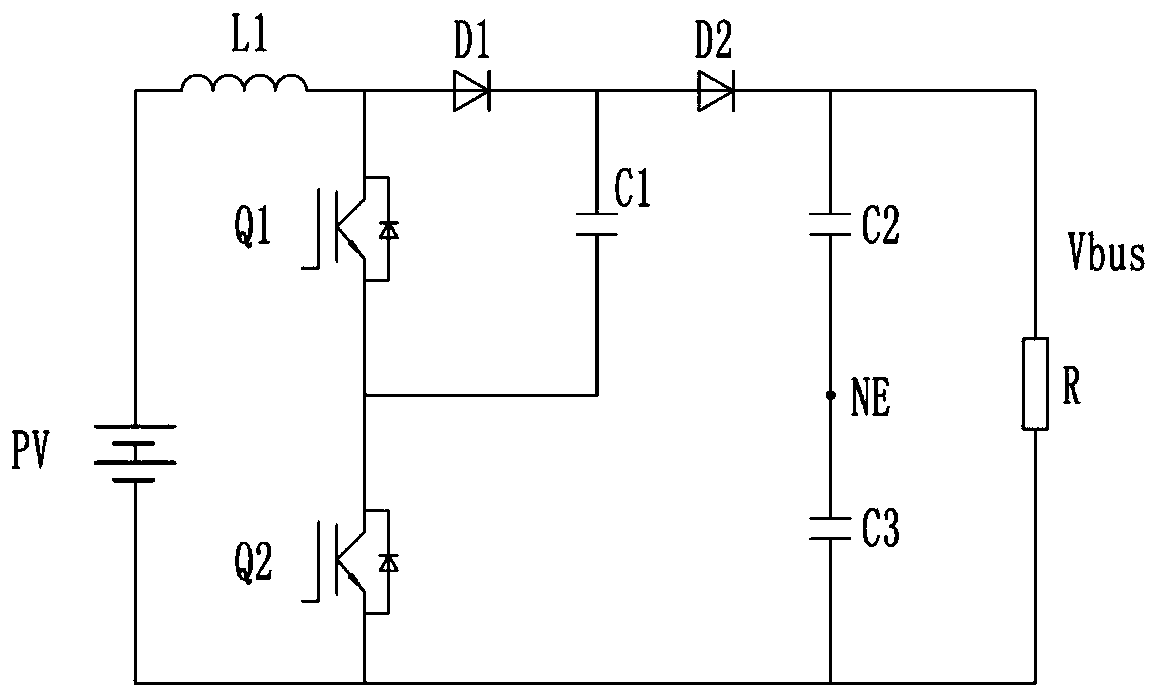
[0067] refer to figure 2 , Embodiment 1 of the present invention provides a three-level boost circuit, which has an input terminal and an output terminal. The input end includes a first input end and a second input end, and the output end includes a first output end and a second output end.
[0068] Generally speaking, the boost circuit of this embodiment can be used in various application scenarios, so its input terminal can be coupled with various power input devices to receive power input therefrom. In each embodiment of the present invention, the application scenario in the field of photovoltaic power generation is used as an example for introduction. Therefore, the input terminal of the boost circuit is coupled to the photovoltaic module PV1, which converts light energy into DC power and then inputs it to the boost circuit. Boost for efficient use of light energy. The positive pole of the photovoltaic module PV1 is connected to the first input terminal, and the negativ...
Embodiment 2-6
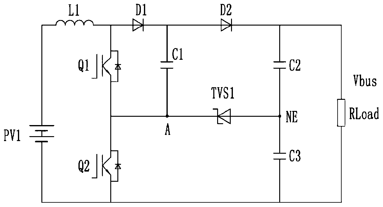
[0090] refer to Figure 3-7 , which respectively correspond to Embodiments 2-6 of the present invention, which are all improved on the basis of Embodiment 1, aiming at solving the problem that after Embodiment 1 introduces the first TVS tube TVS1 configured as a unidirectional TVS tube, Because it is equivalent to an ordinary diode when it works in the forward direction, under the condition of low input voltage, the midpoint voltage of the bus can be transmitted to the input terminal through the body diode of the first TVS transistor TVS1 and the first controllable switch Q1, which is easy to cause the The problem of electric shock accidents.
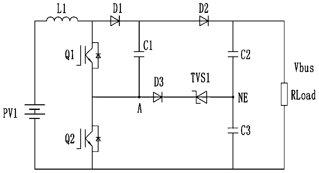
[0091] image 3 In the illustrated embodiment 2, the fourth branch is further provided with a third diode D3, the cathode of which is connected to the cathode of the first TVS transistor TVS1, and the anode of which constitutes the first end of the fourth branch. In the case of the low input voltage, through the reverse cut-off of the...
Embodiment 7-8
[0096] refer to Figure 8-9 , which respectively correspond to Embodiment 7-8 of the present invention, which are all in image 3 The improvement on the basis of the illustrated embodiment 2 aims to solve the problem that the second diode D2 is easily broken down under the condition of low input voltage.
[0097] It can be seen that the circuit further includes a fifth branch on which a fourth diode D4 is arranged, for the input voltage between the first input terminal and the second input terminal is lower than the start-up voltage of the booster circuit When , that is, in the case of the low input voltage, the common point of the first diode D1 and the second diode D2 is clamped.
[0098] One end of the fifth branch is connected to the common point of the first diode D1 and the second diode D2, and the other end can be connected to the second end of the fourth branch, or can be connected to the first diode D2. A common point of the TVS transistor TVS1 and the third diode D...
PUM
 Abstract
Description
Claims
Application Information
 - R&D
- Intellectual Property
- Life Sciences
- Materials
- Tech Scout
- Unparalleled Data Quality
- Higher Quality Content
- 60% Fewer Hallucinations
Browse by: Latest US Patents, China's latest patents, Technical Efficacy Thesaurus, Application Domain, Technology Topic, Popular Technical Reports.
© 2025 PatSnap. All rights reserved.Legal|Privacy policy|Modern Slavery Act Transparency Statement|Sitemap|About US| Contact US: help@patsnap.com