Light broadband multi-frequency-band strong-absorption double-layer structure honeycomb wave-absorbing plate and preparation method thereof

A double-layer structure and multi-band technology, applied in the field of microwave-absorbing materials, can solve the problems of narrow absorbing frequency band, low absorbing intensity and complicated process of honeycomb absorbing board, and achieve low cost, broaden the absorbing frequency band and simple process Effect

Inactive Publication Date: 2020-04-10
AEROSPACE SCI & IND WUHAN MAGNETISM ELECTRON
View PDF4 Cites 17 Cited by
  • Summary
  • Abstract
  • Description
  • Claims
  • Application Information

AI Technical Summary

Problems solved by technology

[0005] The method for preparing a honeycomb wave-absorbing board in the prior art includes: 1) dipping or spraying a kind of wave-absorbing coating on the surface of a single-layer honeycomb, and the prepared honeycomb wave-absorbing board has the characteristics of narrow wave-absorbing frequency band or low wave-absorbing intensity; 2) The multi-layer absorbing honeycomb structure can improve the absorbing intensity and broaden the absorbing frequency band, but it has the characteristics of complicated process and increased cost.

Method used


Image

  • Light broadband multi-frequency-band strong-absorption double-layer structure honeycomb wave-absorbing plate and preparation method thereof
  • Light broadband multi-frequency-band strong-absorption double-layer structure honeycomb wave-absorbing plate and preparation method thereof
  • Light broadband multi-frequency-band strong-absorption double-layer structure honeycomb wave-absorbing plate and preparation method thereof

Examples


preparation example Construction

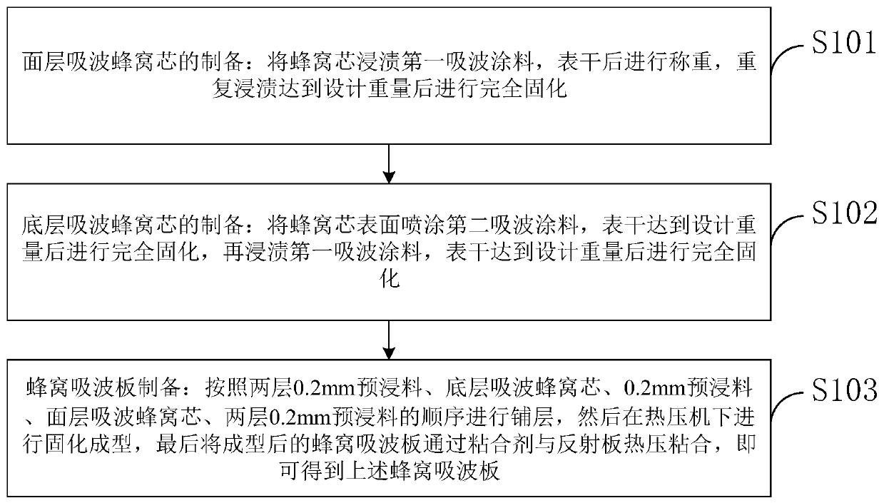
[0046] like image 3 As shown, the preparation method of the light-weight broadband multi-band strong absorption double-layer structure honeycomb wave absorbing board provided by the embodiment of the present invention includes the following steps:

[0047] S3101: Preparation of surface-layer wave-absorbing honeycomb core: Immerse the honeycomb core with the first wave-absorbing paint, weigh it after it is dry, repeat the dipping to reach the designed weight, and then fully cure.

[0048] S102: Preparation of the bottom wave absorbing honeycomb core: spray the second wave absorbing paint on the surface of the honeycomb core, fully cure after the surface dryness reaches the design weight, and then immerse the first wave absorbing paint, and completely cure after the surface dryness reaches the design weight.

[0049] S103: Preparation of honeycomb wave-absorbing board: Lay up in the order of two layers of 0.2mm prepreg, bottom layer of wave-absorbing honeycomb core, 0.2mm prepr...

Embodiment 1

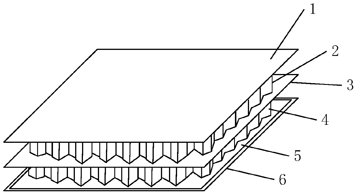
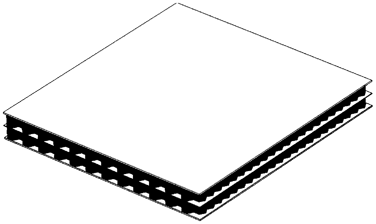
[0055] The invention provides a light-weight broadband multi-band strong absorption double-layer structure honeycomb wave-absorbing board, comprising an upper layer skin, a surface layer wave-absorbing honeycomb core, an adhesive layer, a bottom layer wave-absorbing honeycomb core, a bottom layer skin and a reflection layer. The structure of the absorbing board is 0.4mm surface skin, 10.5mm surface absorbing honeycomb core, 0.2mm middle bonding layer, 10.5mm bottom absorbing honeycomb core, 0.4mm bottom skin, and 0.4mm carbon fiber board reflection layer.

[0056] The areal density of the honeycomb structure wave-absorbing plate material prepared above is 5.5kg / m 2 , the average value in the range of 1GHz-4GHz≤-7dB, the average value in the range of 4GHz-12GHz≤-13.8dB, the average value in the range of 12GHz-18GHz, 26.5GHz-40GHz≤-17.4dB.

Embodiment 2

[0058] The invention provides a light-weight broadband multi-band strong absorption double-layer structure honeycomb wave-absorbing board, comprising an upper layer skin, a surface layer wave-absorbing honeycomb core, an adhesive layer, a bottom layer wave-absorbing honeycomb core, a bottom layer skin and a reflection layer. The structure of the absorbing board is 0.4mm surface skin, 11mm surface absorbing honeycomb core, 0.2mm middle bonding layer, 11mm bottom absorbing honeycomb core, 0.4mm bottom skin, and 0.4mm carbon fiber board reflection layer.

[0059] The areal density of the honeycomb structure wave-absorbing plate material prepared above is 5.8kg / m 2 , the average value in the range of 1GHz-4GHz≤-7.5dB, the average value in the range of 4GHz-12GHz≤-13.3dB, the average value in the range of 12GHz-18GHz, 26.5GHz-40GHz≤-17.3dB.


PUM

PropertyMeasurementUnit
electrical bandwidthaaaaaaaaaa

Abstract

The invention belongs to the technical field of wave-absorbing materials, and discloses a light broadband multi-frequency-band strong-absorption double-layer structure honeycomb wave-absorbing plate and a preparation method thereof. The light broadband multi-frequency-band strong-absorption double-layer structure honeycomb wave-absorbing plate is sequentially provided with an upper-layer skin, a surface-layer wave-absorbing honeycomb core, a bonding layer, a bottom-layer wave-absorbing honeycomb core, a bottom-layer skin and a reflecting layer from top to bottom, wherein various layers are adhered, the surface of the surface-layer wave-absorbing honeycomb core is dipped with a first wave-absorbing coating material, the surface of the bottom-layer wave-absorbing honeycomb core is sprayed with a second wave-absorbing coating material, and the outer side of the second wave-absorbing coating material is dipped with the first wave-absorbing coating material. According to the invention, honeycomb is sprayed and dipped with the wave-absorbing coating material, and the impedance matching design is carried out on the upper-layer skin, the surface-layer wave-absorbing honeycomb, the bottom-layer wave-absorbing honeycomb, the bottom-layer skin and the reflecting layer, so that the wave-absorbing strength is further improved and the wave-absorbing frequency band is widened under the condition of meeting the environmental use requirements so as to widen the frequency band of the honeycomb wave-absorbing plate and improve the absorption peak strength of the honeycomb wave-absorbing plate.

Description

technical field [0001] The invention belongs to the technical field of wave absorbing materials, and in particular relates to a light-weight broadband multi-band strong absorption double-layer structure honeycomb wave absorbing board and a preparation method thereof. Background technique [0002] As one of the important materials for the application of weapons and equipment, radar absorbing materials have always been a focus of the frontier of national defense science and technology. They can reduce the reflection and scattering of electromagnetic waves through their own absorption and attenuation, so as to achieve the loss of electromagnetic waves and greatly reduce the target. Radar Scattering Interface (RSC) to improve its survivability, defense and overall combat capability. [0003] Radar absorbing materials can be divided into coating type and structural type according to the material forming process and bearing capacity. Structural radar absorbing material is a kind o...

Claims


Application Information

Patent Timeline
Patent Type & Authority Applications(China)
IPC IPC(8): B32B27/34B32B27/02B32B27/06B32B27/12B32B9/00B32B9/04B32B5/02B32B15/20B32B15/04B32B3/12B32B7/12B32B7/08B32B33/00B32B37/12B32B37/10B32B37/06B32B37/24B32B38/08C09D5/32
CPCB32B3/12B32B5/02B32B5/26B32B7/08B32B7/12B32B15/04B32B15/20B32B33/00B32B37/06B32B37/10B32B37/1284B32B37/24B32B38/08B32B2037/243B32B2255/02B32B2255/10B32B2255/20B32B2255/205B32B2260/021B32B2260/04B32B2262/0269B32B2262/106B32B2305/024B32B2307/212C09D5/32
Inventor 明鹏王玉成彭学刚尹生汪均鉴王绪超王俊鹏
Owner AEROSPACE SCI & IND WUHAN MAGNETISM ELECTRON
Why Eureka
Try Eureka