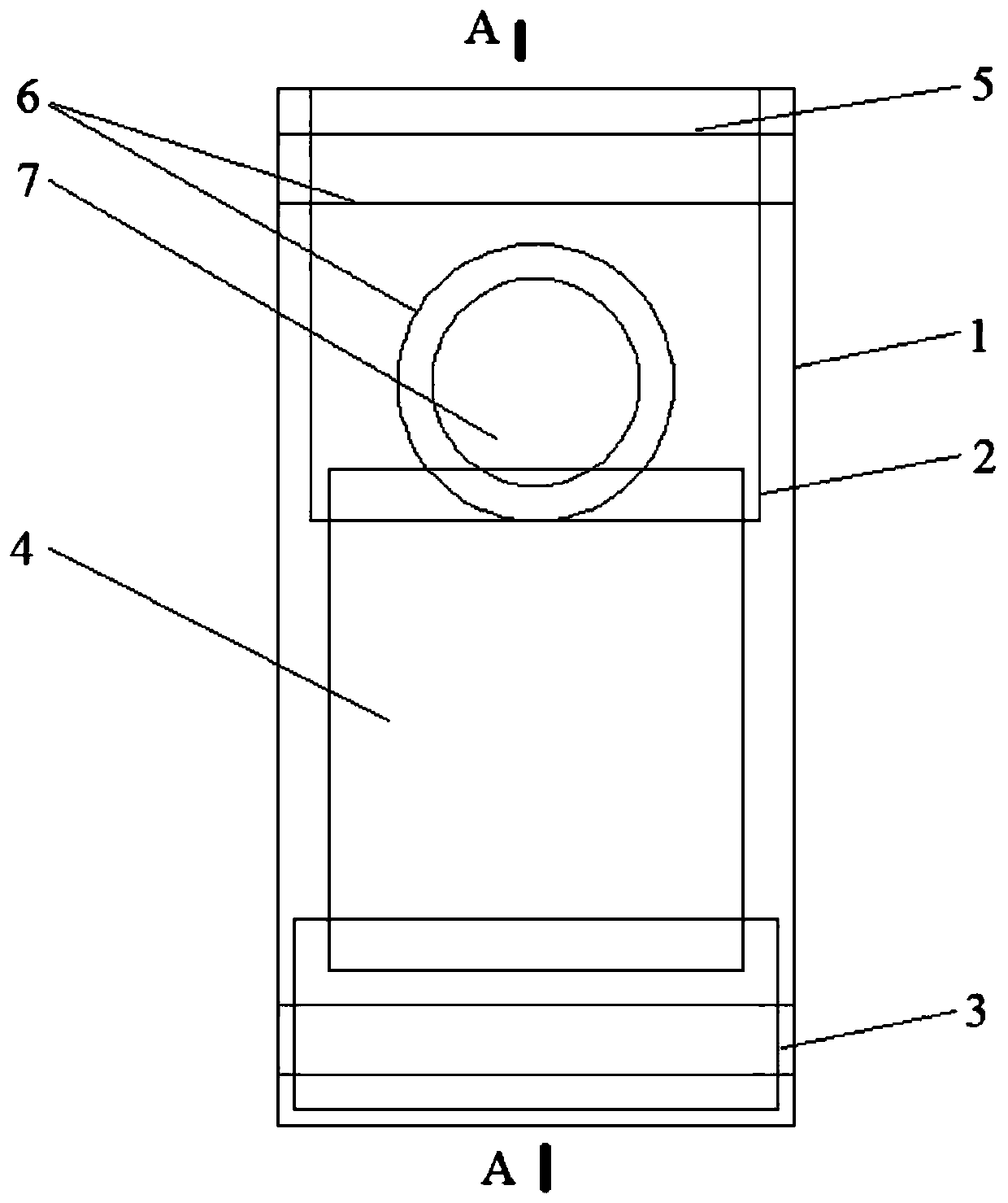
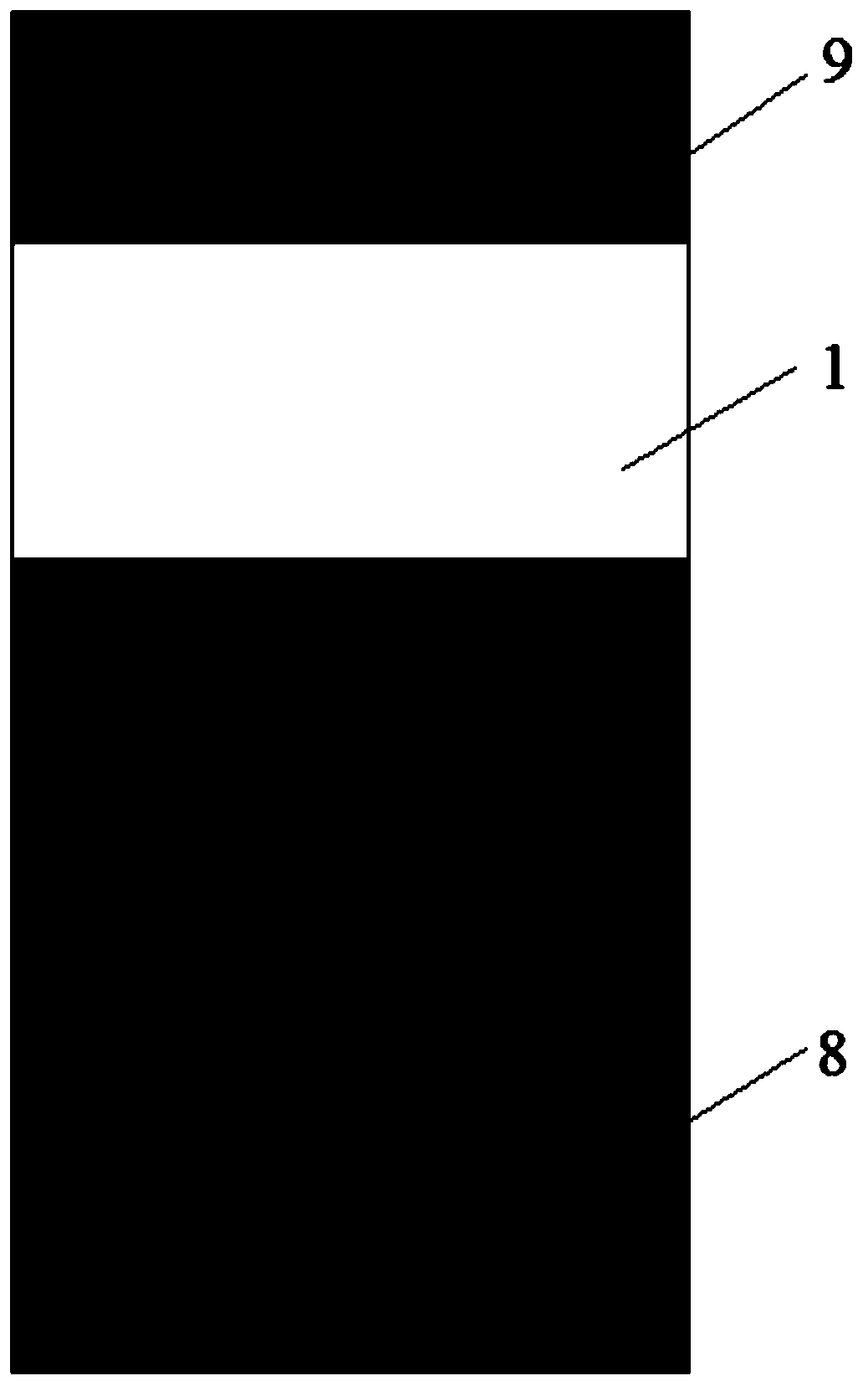
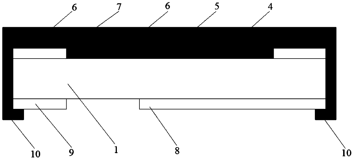
Surface-mounted 5G communication loading sheet and preparation method thereof
A surface-mounted, load chip technology, applied in the direction of electrical components, circuits, waveguide devices, etc., can solve problems such as difficult matching of software and hardware, and achieve the effect of improving radio frequency performance and increasing capacitance
- Summary
- Abstract
- Description
- Claims
- Application Information
AI Technical Summary
Problems solved by technology
Method used
Image
Examples
specific Embodiment 1
[0084] The preparation method of the load sheet 1 for 5G communication comprises the following steps:
[0085] S1, cleaning the substrate: select an aluminum nitride ceramic substrate with a size of 1.5×3.0×0.385mm, and use more than 95vol.% alcohol to clean the surface of the aluminum nitride ceramic substrate. printing;
[0086] S2, printing the front circuit and grounding wire: adopt the thick film printing process, use the silver paste 1 to carry out screen printing through the screen plate with a tension of 25±1N at 25±2°C, and use nitrogen after the treatment of step S1 The front side of the aluminum ceramic substrate is printed with the front circuit and the ground wire. After the printing is completed, it is left to stand for 15 minutes, pre-baked at 165°C for 20 minutes, and high-temperature sintered at 850°C for 15 minutes to form a cured front circuit and ground wire;
[0087] S3, printed resistors: use screen printing process, select 400 mesh steel screen, use res...
specific Embodiment 2
[0096] The preparation steps of the carrier sheet 2 for 5G communication are as described in the specific example 1. The difference is:
[0097] Silver paste 2 is used in step S2 and step S8, and the process after printing is as follows: after printing, stand for 20 minutes, pre-bake at 170°C for 15 minutes, and high-temperature sintering at 860°C for 17 minutes.
[0098] In step S3, resistive paste 2 is used, and the selected steel screen is 420 mesh, and the process after printing is as follows: after the printing is completed, stand for 10 minutes, pre-bake at 175°C for 15 minutes, and high-temperature sintering at 800°C for 20 minutes.
[0099] In step S5, step S6 and step S7, the process after printing is as follows: after printing, place it for 23 minutes, then pre-bake it at 105°C for 20 minutes until the surface is dry, and then bake it at 210°C for 60 minutes until it is completely dry .
[0100] The size of the 5G communication load sheet 2 prepared above is 1.5×3....
PUM
| Property | Measurement | Unit |
|---|---|---|
| Diameter | aaaaa | aaaaa |
| Viscosity | aaaaa | aaaaa |
| Diameter | aaaaa | aaaaa |
Abstract
Description
Claims
Application Information


