Supercharge Your Innovation With Domain-Expert AI Agents!

Printed circuit board

A printed circuit board and outer layer circuit technology, applied in the directions of printed circuit, printed circuit, printed circuit manufacturing, etc., can solve the problems of increasing the unit cost of the product and difficulty in forming through holes, so as to reduce the unit cost of the product and reduce the overall thickness. Effect

Active Publication Date: 2020-04-10
LG INNOTEK CO LTD
View PDF7 Cites 0 Cited by
  • Summary
  • Abstract
  • Description
  • Claims
  • Application Information

AI Technical Summary

Problems solved by technology

[0015] In addition, since the outer layer circuit pattern has a protruding structure in a conventional printed circuit board, a passivation layer should be formed using a thermosetting epoxy resin such as a solder resist to protect the surface of the outer layer circuit pattern on the outermost layer of the substrate, and thus, There is a problem that the unit cost of the product increases
[0016] Also, in conventional printed circuit boards, since the insulating layer is made using a thermosetting resin with glass fibers, it is difficult to form via holes for connecting the layers

Method used


Image

  • Printed circuit board
  • Printed circuit board
  • Printed circuit board

Examples


Embodiment Construction

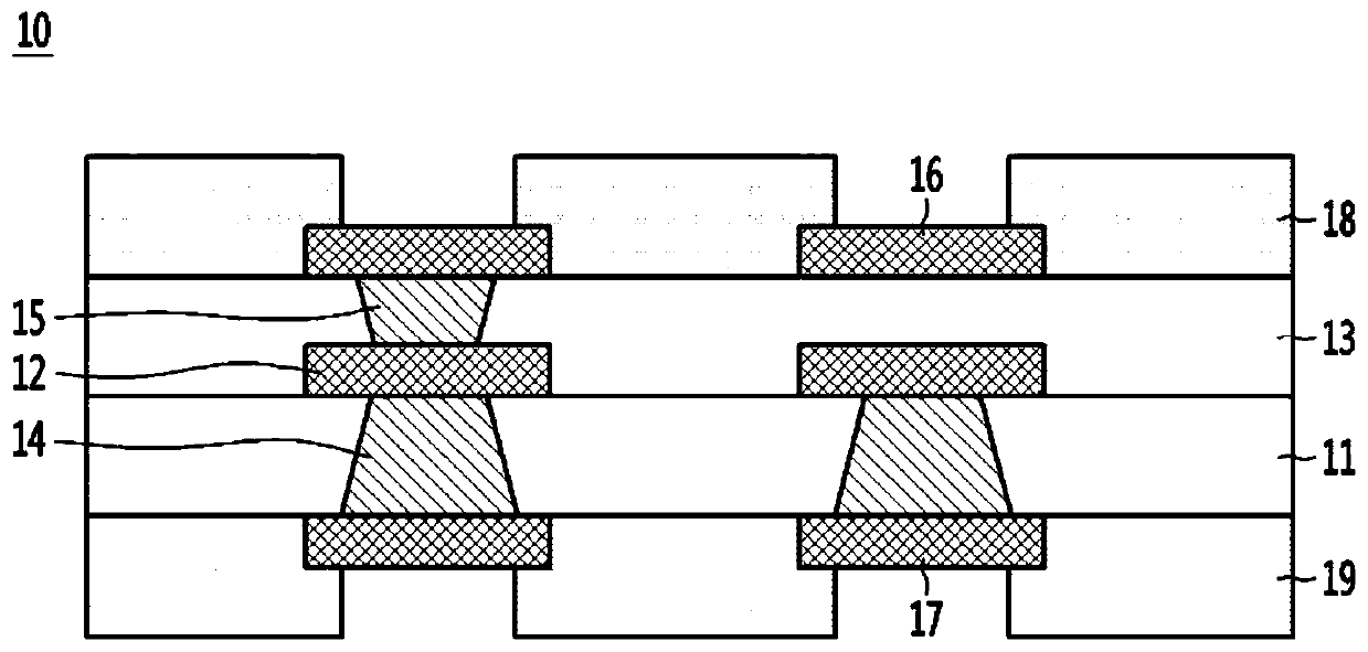
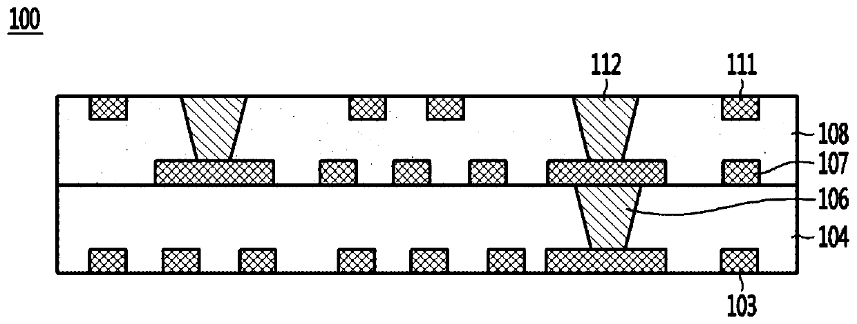
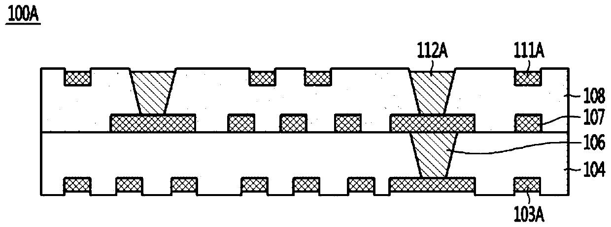
[0053] Hereinafter, embodiments disclosed in this specification will be described in detail with reference to the accompanying drawings, but the same or similar components are denoted by the same reference numerals regardless of the reference numerals, and repeated description thereof will be omitted. The component suffixes 'module' and 'part' used in the following description are given or mixed together only in consideration of ease of authoring the description, and do not have meanings or roles to distinguish from each other. In addition, in describing the embodiments disclosed in this specification, when it is determined that the detailed description of related well-known technologies unnecessarily obscures the gist of the embodiments disclosed in this specification, its detailed description will be omitted. In addition, the drawings are only used to facilitate the understanding of the embodiments disclosed in this specification, and the technical scope disclosed in this spe...


PUM


Abstract

A printed circuit board according to an embodiment of the present invention comprises: a first insulating layer; an inner layer circuit pattern disposed on an upper surface of the first insulating layer; a second insulating layer, disposed on the first insulating layer, for covering the inner layer circuit pattern; a first outer layer circuit pattern embedded in a lower surface of the first insulating layer; and a second outer layer circuit pattern embedded in an upper surface of the second insulating layer, wherein the first insulating layer comprises a thermosetting resin, and the second insulating layer comprises a photocurable resin.

Description

technical field [0001] The present invention relates to a printed circuit board (PCB), and more particularly, to a PCB including circuit patterns buried on both sides thereof and a method of manufacturing the PCB. Background technique [0002] A printed circuit board (PCB) is a circuit board that electrically connects or mechanically fixes certain electronic components, and is composed of a copper foil layer attached to an insulating layer such as phenol resin, epoxy resin, etc. to form a predetermined wiring pattern. [0003] Such printed circuit boards are generally classified according to the number of layers into single-sided printed circuit boards in which wiring is formed on only one side of the insulating layer, double-sided printed circuit boards in which wiring is formed on both sides of the insulating layer, and multi-layered printed circuit boards. Multilayer printed circuit board with wiring. [0004] Among them, multilayer printed circuit boards are made by imp...

Claims


Application Information

Patent Timeline
Patent Type & Authority Applications(China)
IPC IPC(8): H05K3/10H05K1/03H05K3/28H05K3/46
CPCH05K3/4682H05K2201/0376H05K1/115H05K2201/096H05K3/428H05K2201/0195H05K3/107H05K1/0306H05K3/28H05K3/4623H05K1/0298H05K1/0313H05K3/465H05K2201/0209H05K2201/09563
Inventor 申铉乾
Owner LG INNOTEK CO LTD
Features
  • R&D
  • Intellectual Property
  • Life Sciences
  • Materials
  • Tech Scout
  • Unparalleled Data Quality
  • Higher Quality Content
  • 60% Fewer Hallucinations
Learn More