
Biological recognition module and preparation method thereof

A biometric identification and chip technology, applied in the field of biometric identification modules and their preparation, can solve problems such as easily damaged biometric identification chip functional areas, and achieve the effects of ensuring sensitive work, accurate alignment, and optimized thickness

Active Publication Date: 2020-04-17
YUNNAN SECURITY TECH
View PDF7 Cites 1 Cited by
  • Summary
  • Abstract
  • Description
  • Claims
  • Application Information

AI Technical Summary

Problems solved by technology

During the use of the existing biometric identification module, the functional area of ​​the biometric identification chip is easily damaged under the action of pressing force due to the long-term pressing of the biometric identification module

Method used


Image

  • Biological recognition module and preparation method thereof
  • Biological recognition module and preparation method thereof
  • Biological recognition module and preparation method thereof

Examples


Embodiment Construction

[0017] Such as Figure 1-Figure 9 Shown, a kind of preparation method of biological recognition module comprises the following steps:

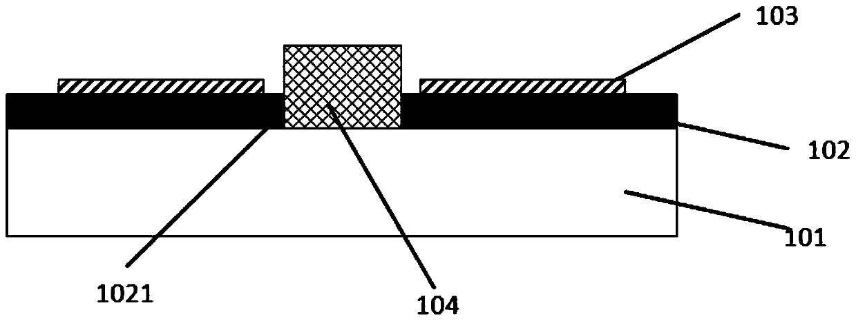
[0018] Such as figure 1 As shown, in step 1), a substrate 101 is provided, and the substrate has an opposite first surface and a second surface; in step 2), a first dielectric layer is formed on the first surface of the substrate 101 102 , forming a conductive wiring layer 103 on the first dielectric layer 102 .

[0019] Wherein, the material of the substrate 101 is glass, ceramics, plastic or silicon. The material of the first dielectric layer 102 is one or more of silicon nitride, silicon oxynitride, silicon oxide, silicon carbide, aluminum oxide, aluminum nitride, and the first dielectric layer 102 can be a single layer or multi-layer structure, the preparation method of the first dielectric layer 102 is PECVD method, ALD method or thermal oxidation method, and the material of the conductive wiring layer 103 is one of gold, silver, coppe...


PUM

PropertyMeasurementUnit
thicknessaaaaaaaaaa
thicknessaaaaaaaaaa
thicknessaaaaaaaaaa

Abstract

The invention relates to a biological recognition module and a preparation method thereof. The method comprises the steps of: providing a substrate with a first surface and a second surface which areopposite to each other, and forming a first dielectric layer and a conductive wiring layer on the first surface of the substrate, forming a slotted region in the first dielectric layer, and then embedding an elastic buffer layer in the slotted region, providing a carrier plate, setting a release film and a biological recognition chip on the carrier plate, forming a metal retaining wall structure at the periphery of a bonding pad of the biological recognition chip through a photoetching process, arranging solder balls in an area, corresponding to the bonding pads, in the conductive wiring layer, then setting the biological recognition chip on the conductive wiring layer, enabling the elastic buffer layer to be in contact with the biological recognition chip, and melting the solder balls through a reflow soldering process to be embedded into the corresponding metal retaining wall structures, forming a plastic package layer on the substrate and forming a conductive column in the plastic package layer, and finally, thinning the substrate.

Description

technical field [0001] The invention relates to the field of semiconductor packaging, in particular to a biometric identification module and a preparation method thereof. Background technique [0002] In the existing biometric identification module, usually a hard encapsulation material layer is formed on the biometric identification chip, then the encapsulation material layer is thinned, and then a protective cover is provided on the thinned encapsulation material layer. During the use of the existing biometric identification module, since the biometric identification module is pressed many times for a long time, the functional area of ​​the biometric identification chip is easily damaged under the action of the pressing force. Contents of the invention [0003] The purpose of the present invention is to overcome the deficiencies of the above-mentioned prior art, and provide a biometric identification module and a preparation method thereof. [0004] In order to achieve ...

Claims


Application Information

Patent Timeline
Patent Type & Authority Applications(China)
IPC IPC(8): H01L21/50H01L21/56H01L21/60H01L23/31H01L23/488
CPCH01L21/50H01L21/56H01L23/3114H01L23/488H01L24/81H01L2224/81007H01L2224/81051H01L2224/8121H01L2224/16225
Inventor 王桥
Owner YUNNAN SECURITY TECH
Learn More