Charge pump circuit for delay-locked loop
A delay-locked loop and charge pump technology, applied in the field of microelectronics, can solve problems affecting the performance characteristics of delay-locked loops, current mismatch, charge sharing, etc.
- Summary
- Abstract
- Description
- Claims
- Application Information
AI Technical Summary
Problems solved by technology
Method used
Image
Examples
Embodiment
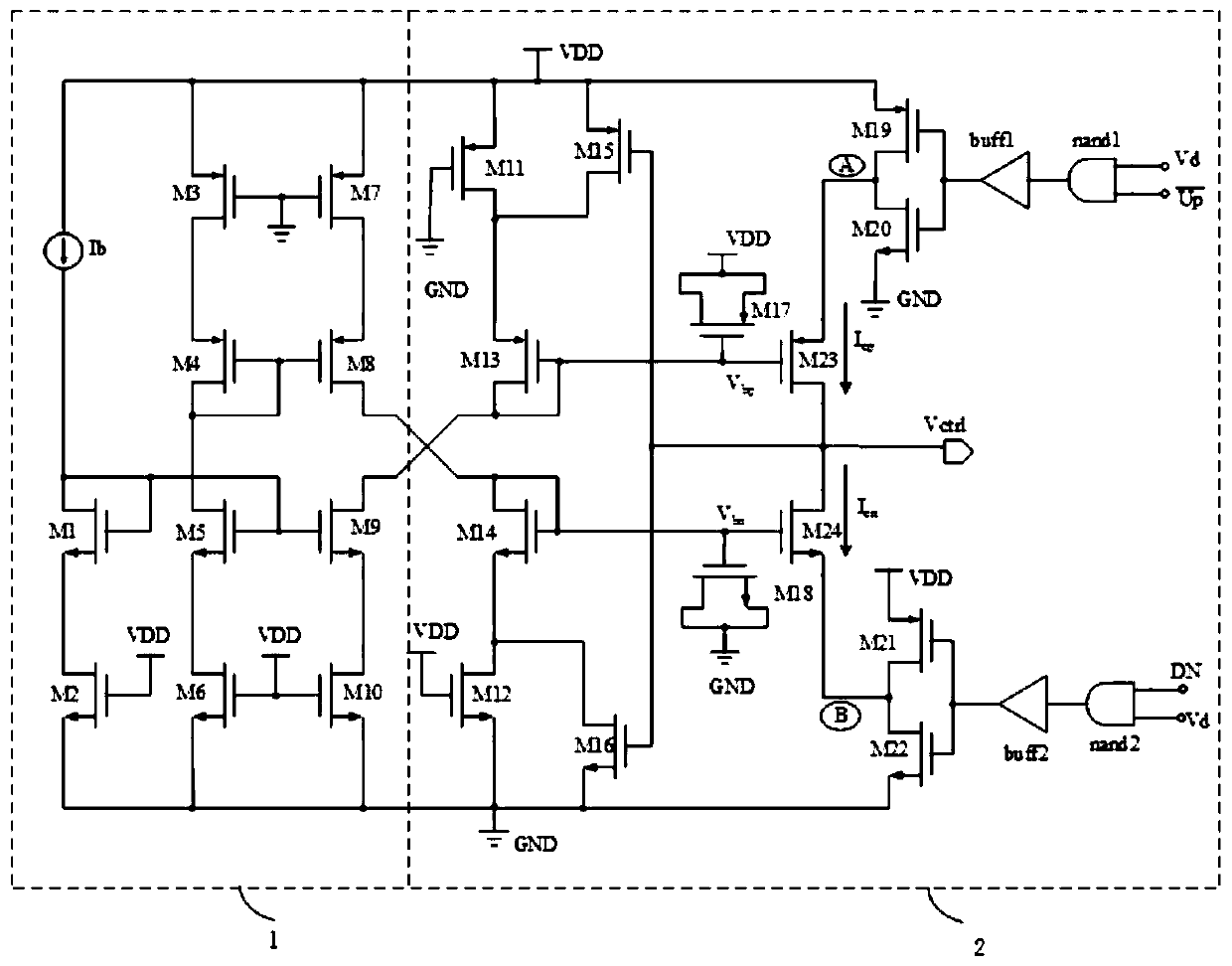
[0023] A charge pump circuit for a delay locked loop such as figure 2 As shown, it includes a charge and discharge current bias circuit 1 and a charge pump core circuit 2; wherein, the signal output of the charge and discharge current bias circuit 1 is connected to the signal input terminal of the charge pump core circuit 2; the charge and discharge The current bias circuit 1 provides a bias signal for the charge pump core circuit 2 .
[0024] The current mirrors of the charge and discharge current bias circuit 1 all adopt a current mirror structure that operates in a linear region MOS transistor as source negative feedback impedance to improve current accuracy; the charge pump core circuit 2 adopts the gate of the NMOS transistor M20 and the PMOS The gate of the transistor M19 is connected and the source of the NMOS transistor M20 is connected to the external ground GND structure to suppress the charge sharing effect between the parasitic capacitance of node A and the capaci...
PUM
 Abstract
Description
Claims
Application Information
 - R&D Engineer
- R&D Manager
- IP Professional
- Industry Leading Data Capabilities
- Powerful AI technology
- Patent DNA Extraction
Browse by: Latest US Patents, China's latest patents, Technical Efficacy Thesaurus, Application Domain, Technology Topic, Popular Technical Reports.
© 2024 PatSnap. All rights reserved.Legal|Privacy policy|Modern Slavery Act Transparency Statement|Sitemap|About US| Contact US: help@patsnap.com


