Digital alloy based back barrier for p-channel nitride transistors

A nitride, back-barrier technology, used in semiconductor devices, semiconductor/solid-state device manufacturing, electrical components, etc., can solve problems such as lattice mismatch and growth of thick analog AlGaN

Pending Publication Date: 2020-04-17
HRL LAB
View PDF14 Cites 0 Cited by
  • Summary
  • Abstract
  • Description
  • Claims
  • Application Information

AI Technical Summary

Problems solved by technology

However, thick simulated AlGaN with high Al content

Method used


Image

  • Digital alloy based back barrier for p-channel nitride transistors
  • Digital alloy based back barrier for p-channel nitride transistors
  • Digital alloy based back barrier for p-channel nitride transistors

Examples


Embodiment Construction

[0043] It should be understood at the outset that although exemplary embodiments are shown below, the technology may be implemented using any number of techniques, whether currently known or not. The technology should by no means be limited to the exemplary embodiments, figures and techniques described below. Additionally, the drawings are not necessarily drawn to scale.

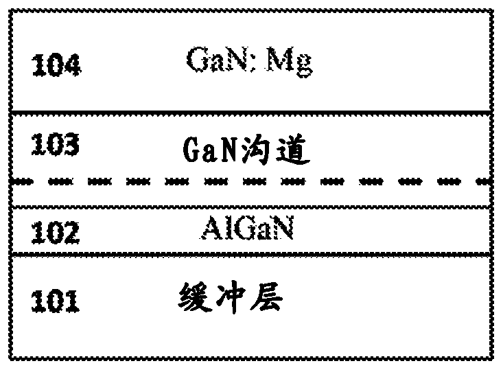
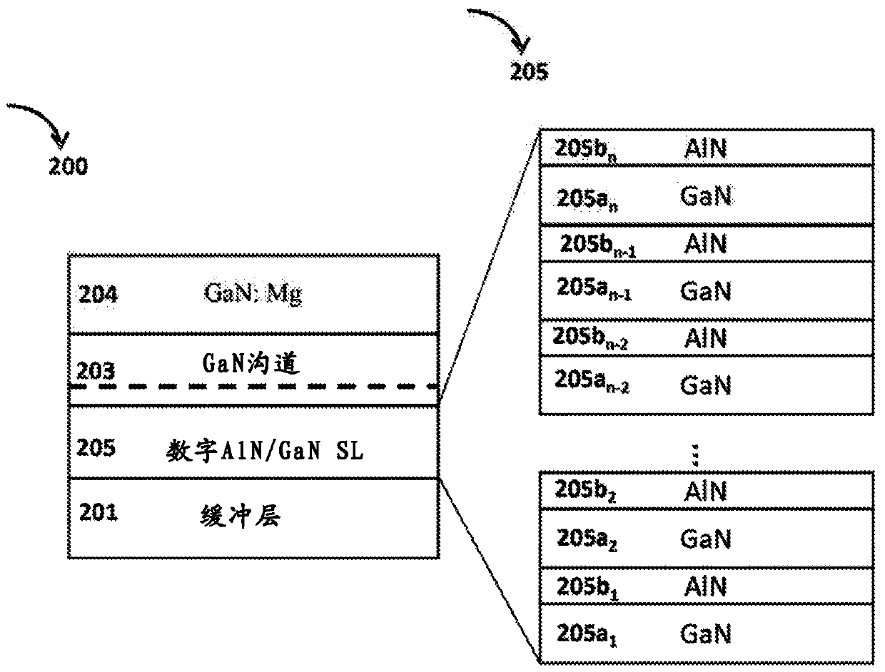
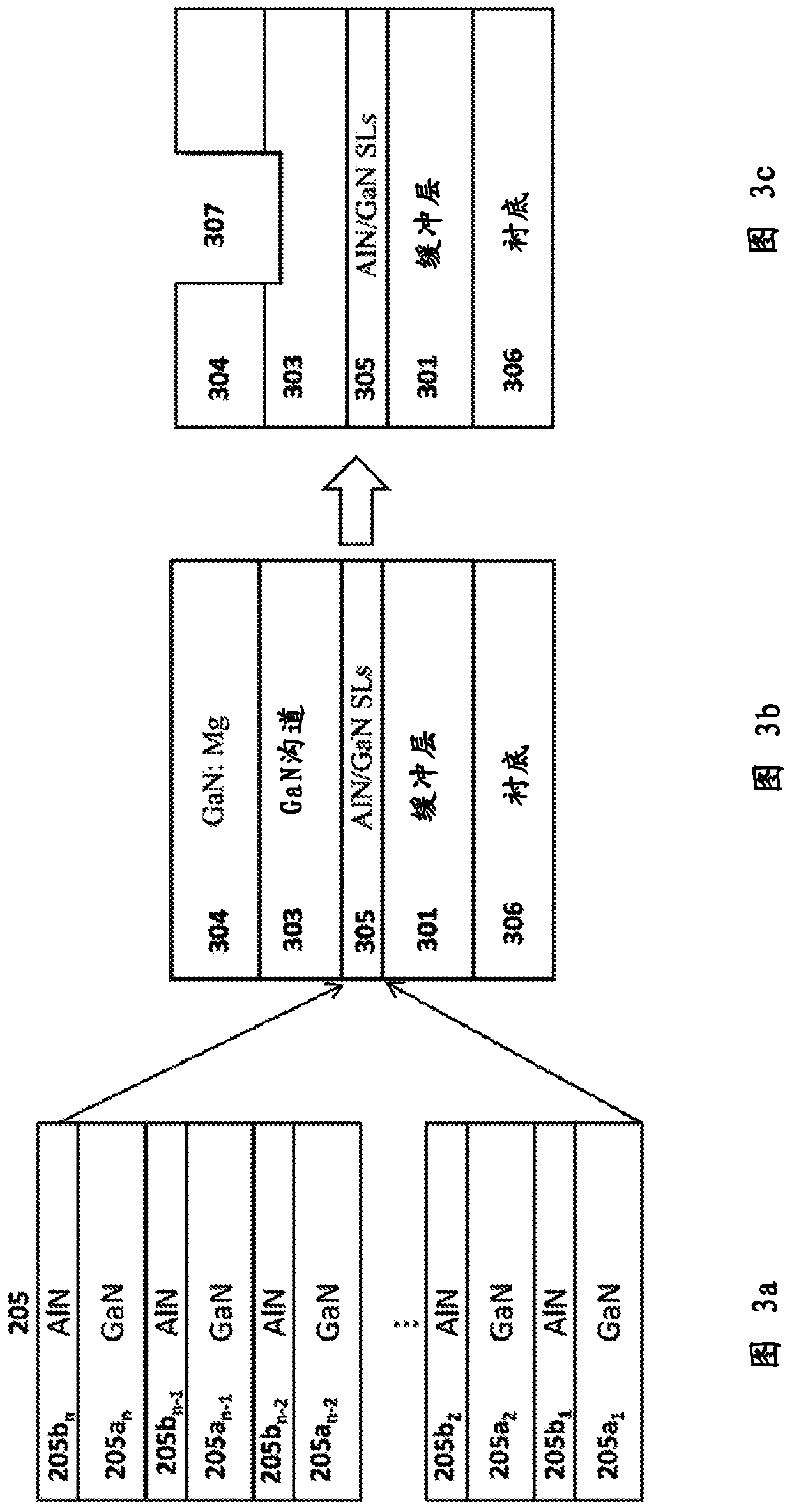
[0044] Recently, GaN transistors have revolutionized high-power and high-speed switching electronics, and application demands continue to drive higher and higher power-handling capabilities. The power handling capability of a GaN transistor is directly dependent on the channel conductivity.

[0045] Group III nitride semiconductor materials (aluminum, indium, gallium) nitrides are excellent wide bandgap semiconductors well suited for modern electronic and optoelectronic applications. Although the present invention describes techniques using GaN, the presented techniques are applicable to any Ill-nitride se...


PUM

PropertyMeasurementUnit
Thicknessaaaaaaaaaa

Abstract

A III-nitride power handling device and the process of making the III-nitride power handling device are disclosed that use digital alloys as back barrier layer to mitigate the strain due to lattice mismatch between the channel layer and the back barrier layer and to provide increased channel conductivity. An embodiment discloses a GaN transistor using a superlattice binary digital alloy as back barrier comprising alternative layers of AlN and GaN. Other embodiments include using superlattice structures with layers of GaN and AlGaN as well as structures using AlGaN/AlGaN stackups that have different Aluminum concentrations. The disclosed device has substantially increased channel conductivity compared to traditional analog alloy back barrier devices.

Description

technical field [0001] The present invention relates generally to the field of III-nitride transistors, and more particularly to the design and fabrication of P-channel GaN transistors. Background technique [0002] GaN power integrated circuits (ICs) have the potential to significantly reduce the size and weight of power electronic systems, thereby significantly reducing the cost of power electronics. P-channel GaN transistors are key components in the fabrication of GaN power ICs. Such power electronics systems are widely required in electric / hybrid vehicles, more electric aircraft, and many consumer electronics. [0003] A variety of GaN transistors are known, and they include P-channel transistors as well as N-channel transistors that use analog alloys to improve conductivity. The use of ternary alloys such as AlGaN (aluminum gallium nitride) is commonly referred to in the art as analog alloys. To increase the power handling capability of GaN transistors, several tech...

Claims


Application Information

Patent Timeline
IPC IPC(8): H01L29/10H01L29/51H01L21/02
CPCH01L29/2003H01L29/4236H01L29/7781H01L29/155
Inventor 储荣明曹宇
Owner HRL LAB
Why Eureka
Try Eureka