Silicon carbide insulated gate bipolar transistor and manufacturing method thereof

A technology of bipolar transistors and manufacturing methods, applied in semiconductor/solid-state device manufacturing, semiconductor devices, electrical components, etc., can solve problems such as high cost, complicated process, and high difficulty, and achieve increased area, optimized threshold characteristics, and improved reliability effect

Inactive Publication Date: 2020-04-21
INST OF MICROELECTRONICS CHINESE ACAD OF SCI
View PDF5 Cites 5 Cited by
  • Summary
  • Abstract
  • Description
  • Claims
  • Application Information

AI Technical Summary

Problems solved by technology

For this technology, on the one hand, multiple epitaxy is required, and low-resistance thick film epitaxy is required. The process is complex and difficult; The overall preparation process and platform capabilities have higher requirements, the process is complex, difficult and costly

Method used


Image

  • Silicon carbide insulated gate bipolar transistor and manufacturing method thereof
  • Silicon carbide insulated gate bipolar transistor and manufacturing method thereof
  • Silicon carbide insulated gate bipolar transistor and manufacturing method thereof

Examples


Embodiment Construction

[0050] In order to make the object, technical solution and advantages of the present invention clearer, the present invention will be described in further detail below in conjunction with specific embodiments and with reference to the accompanying drawings.

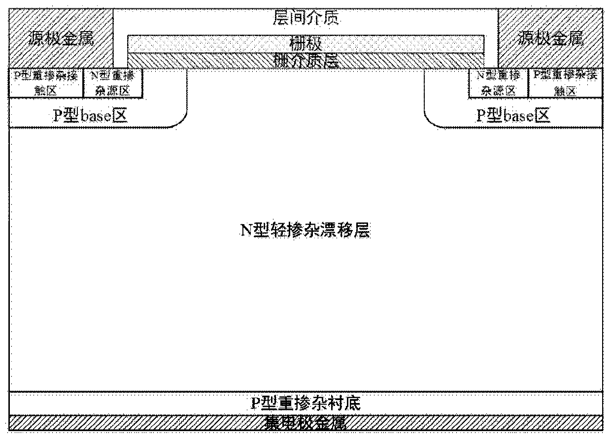
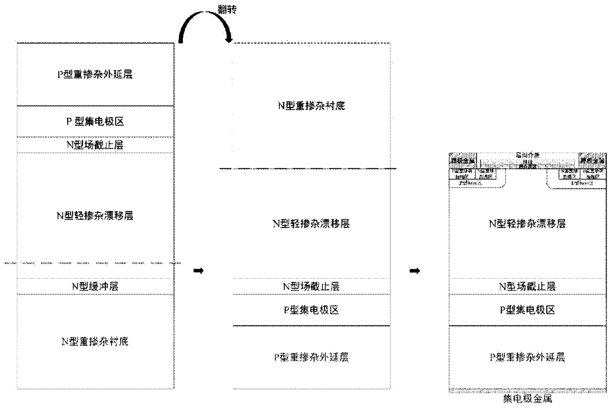
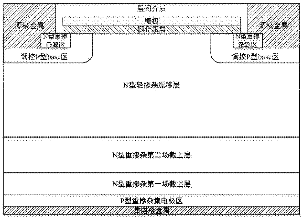
[0051] Such as image 3 As shown, the silicon carbide insulated gate bipolar transistor provided by the embodiment of the present invention includes: N-type heavily doped first field stop layer, N-type heavily doped second field stop layer, N-type lightly doped drift layer, regulating P Type Base region, N-type heavily doped source region, source metal, gate dielectric layer, gate, interlayer dielectric and P-type heavily doped collector region, wherein:

[0052] The N-type heavily doped first field stop layer has a doping concentration of 10 16 to 10 18 cm -3 , with a thickness of 0.5 to 3 μm.

[0053] The N-type heavily doped second field stop layer is formed by epitaxial growth on the N-type heavily doped first field...


PUM

PropertyMeasurementUnit
thicknessaaaaaaaaaa
thicknessaaaaaaaaaa
thicknessaaaaaaaaaa

Abstract

The invention provides a silicon carbide insulated gate bipolar transistor comprising an N-type heavily doped first field stop layer; an N-type heavily doped second field stop layer which is formed onthe N-type heavily doped first field stop layer; an N-type lightly doped drift layer which is formed on the N-type heavily doped second field stop layer; a regulation and control P-type Base region which is formed in the N-type lightly doped drift layer; an N-type heavily doped source region which is formed in the regulation and control P-type Base region; source metal which is formed in the partial region of the regulation and control P-type Base region and the partial upper surface of the N-type heavily doped source region and forms ohmic contact with the upper surface and the side wall ofthe N-type heavily doped source region; a gate dielectric layer which is formed on the N-type lightly doped drift layer; a grid electrode which is formed on the grid dielectric layer; an interlayer dielectric which is formed on the grid electrode and the two sides of the grid electrode so as to isolate the grid electrode from the source metal; and a P-type heavily doped collector region which is formed on the back surface of the N-type heavily doped first field stop layer. The double-layer field stop layer structure is formed so that the characteristics of the device are optimized and the robustness is improved.

Description

technical field [0001] The invention relates to the technical field of manufacturing semiconductor devices, in particular to a silicon carbide insulated gate bipolar transistor and a manufacturing method thereof. Background technique [0002] The third-generation semiconductor material silicon carbide (SiC) has the advantages of large band gap, high critical breakdown field strength, high thermal conductivity and high electron saturation rate, and is very suitable for making high-voltage, high-temperature, high-frequency, high-power semiconductor devices. Due to its conductance modulation effect, silicon carbide insulated gate bipolar transistors have good application prospects and advantages in high-voltage fields such as smart grids, solid-state transformers, and high-voltage transmission. [0003] Silicon carbide insulated gate bipolar transistors have N-channel and P-channel, N-channel IGBT uses P-type doped substrate, and P-channel IGBT uses N-type doped substrate. N-c...

Claims


Application Information

Patent Timeline
Patent Type & Authority Applications(China)
IPC IPC(8): H01L29/06H01L21/331H01L29/739
CPCH01L29/7395H01L29/66068H01L29/0607
Inventor 田晓丽冯旺杨雨陆江白云杨成樾刘新宇
Owner INST OF MICROELECTRONICS CHINESE ACAD OF SCI
Why Eureka
Try Eureka