Lateral SCR device with high maintaining voltage

A high sustaining voltage and device technology, applied in the field of electronic science and technology, can solve problems such as inconsistent bias voltage of the emitter junction, circuit malfunction, burnout, etc., to reduce emission efficiency, improve latch-up resistance, and increase voltage drop Effect

Pending Publication Date: 2020-05-01
UNIV OF ELECTRONICS SCI & TECH OF CHINA
View PDF14 Cites 0 Cited by
  • Summary
  • Abstract
  • Description
  • Claims
  • Application Information

AI Technical Summary

Problems solved by technology

If there is an intersection point between the load line of the power supply and the IV characteristic curve of the device, after the ESD pulse turns on the SCR, the SCR device can maintain the open state under the bias of the circuit power supply, causing the device to latch-up. As a result, the circuit cannot work normally, and even faces the risk of burning
In addition, when the lateral SCR device is turned on, due to the existence of the well resistance, the bias voltage of the emitter junction of the cathode and anode parasitic triode is not consistent, which will lead to the concentration of current on one side, and the wider the junction, the more this phenomenon will be. serious

Method used


Image

  • Lateral SCR device with high maintaining voltage
  • Lateral SCR device with high maintaining voltage
  • Lateral SCR device with high maintaining voltage

Examples


Embodiment 1

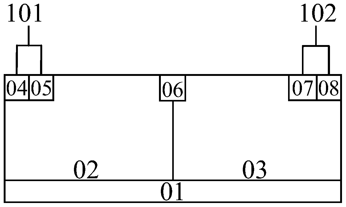
[0027] like figure 2As shown, the high sustain voltage lateral SCR device of this embodiment includes: a P-type substrate 01; an N-type well region 02 tangent to the left edge of the P-type substrate 01 above the inside of the P-type substrate 01; The P-type well region 03 on the upper right side of the bottom 01 is tangent to the N-type well region 02; the anode first N+ contact region 04 is located on the upper side of the N-type well region 02 and is tangent to the left side of the N-type well region 02; The first P+ contact region 05 on the right side of the first N+ contact region 04 and tangent to the first N+ contact region 04 of the anode; N+ low across the two wells is implanted at the junction of the P-type well region 03 and the N-type well region 02 The trigger region 06; the second P+ isolation region 22 of the cathode located above the interior of the P-type well region 03; the second N+ contact region 12 of the cathode located on the right side of the second P+...

Embodiment 2

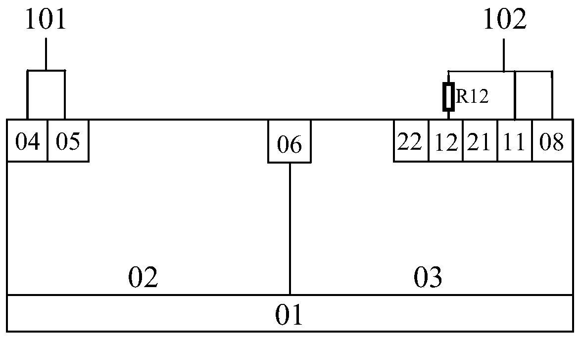
[0032] like Figure 7 As shown, the difference between this embodiment and Embodiment 1 is that: a plurality of cathode N+ contact regions 11, 12, ..., 1n are provided on the left side of the second P+ contact region 08, and multiple cathode N+ contact regions are sequentially inserted between adjacent cathode N+ contact regions. A cathode P+ isolation area 21, 22, ..., 2n, metal contact is formed on the surface of the cathode N + contact area 11, 12, ..., 1n, and one end of the second cathode compensation resistor R13 is connected to the second N + contact area 12 of the cathode, and the other end is connected to the second N + contact area 12 of the cathode. The third N+ contact area 13 of the cathode is connected... One end of the n-1th cathode compensation resistor R1n is connected to the n-1th N+ contact area 1 (n-1) of the cathode, and the other end is connected to the nth N+ contact area 1n of the cathode, and the above n≥ 3.

Embodiment 3

[0034] like Figure 8 As shown, the difference between this embodiment and Embodiment 1 is that the first P+ contact region 05 of the anode of the device is split into two pieces, the first P+ contact region 31 of the anode and the second P+ contact region 32 of the anode, and between the two Insert the first N+ isolation region 41 of the anode, insert the second N+ isolation region 42 of the anode tangent to the second P+ contact region 32 on the right side of the second P+ contact region 32 of the anode; form a metal on the surface of the second P+ contact region 32 of the anode Contact and connect with one end of the first anode compensation resistor R22, the anode first P+ contact region 31 and the surface of the anode first N+ contact region 04 are short-circuited with metal and connected with the other end of the first anode compensation resistor R22 to form the device anode 101.


PUM


Abstract

The invention provides a lateral SCR device with a high maintaining voltage. The device comprises a P-type substrate, an n-type well region, a p-type well region, an anode first N+ contact region, ananode first P+ contact region,, an N+ low trigger region, a cathode second P+ isolation region, a cathode second N+ contact region tangent to the cathode second P+ isolation region, a cathode first P+isolation region tangent to the cathode second N+ contact region, a cathode first N+ contact region tangent to a cathode first P+ isolation region, a second P+ contact region tangent to a cathode first N+ contact region, and a first cathode compensation resistor of which one end is connected with the cathode second N+ contact region, wherein surfaces of the anode first N+ contact region and the anode first P+ contact region are short-circuited by metal to form a device anode, and surfaces of the cathode first N+ contact region and the cathode second P+ contact region are short-circuited through metal and are connected with the other end of the first cathode compensation resistor to form a device cathode. The device is advantaged in that the maintaining voltage of the SCR device is improved, the latch-up resistance of the device is improved, current distribution of a device cathode region is improved, and robustness of the device is improved.

Description

technical field [0001] The invention belongs to the field of electronic science and technology, and is mainly used for electrostatic discharge (Electrostatic Discharge, ESD for short) protection technology. Furthermore, it is a high sustaining voltage SCR device. Background technique [0002] With the development of semiconductor technology and the improvement of integrated circuit technology, the integration level of integrated circuits is getting higher and higher, but at the same time, the impact of electrostatic discharge (ESD, Electrostatic Discharge) on circuits is also increasing. Today, ESD protection has become one of the most important issues for chip designers to consider. [0003] The SCR (silicon controlled rectifier) ​​device has excellent current discharge capability. When used as an ESD protection device, it can greatly reduce the area of ​​the integrated circuit occupied by the ESD module, reduce the cost, and improve the robustness. However, the tradition...

Claims


Application Information

Patent Timeline
Patent Type & Authority Applications(China)
IPC IPC(8): H01L27/02
CPCH01L27/0262H01L27/0296
Inventor 乔明张发备梁龙飞齐钊张波
Owner UNIV OF ELECTRONICS SCI & TECH OF CHINA
Why Eureka
Try Eureka