CMOS image sensor pixel structure with large photosensitive area charge rapid transfer
An image sensor and photosensitive area technology, applied in the direction of electric solid-state devices, circuits, electrical components, etc., can solve the problem of incomplete transfer and transfer speed of photo-generated charges, so as to improve the effective full well capacity, ensure the tailing phenomenon, and reduce the transfer time Effect
- Summary
- Abstract
- Description
- Claims
- Application Information
AI Technical Summary
Problems solved by technology
Method used
Image


Examples
Embodiment Construction
[0012] The present invention will be further described below in conjunction with the accompanying drawings and specific embodiments, but the scope of protection of the present invention is not limited thereto.
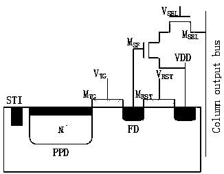
[0013] The CMOS image sensor pixel structure with large photosensitive area and rapid charge transfer can form a lateral electric field inside the PPD by using N-type dopant implantation in the PPD region with multiple concentration gradient changes, shortening the diffusion distance of photogenerated charges during the transfer process. Using this structure can make the charge complete and greatly shorten the transfer time.
[0014] In the process of forming the N-type region of the photodiode, the idea of ion implantation using multiple concentration gradient changes in the lateral direction belongs to the spirit scope of the patent of the present invention.
[0015] In the present invention, the two N-type ion implantations in the photodiode region all use P ions,...
PUM
 Abstract
Description
Claims
Application Information