Film material and preparation method thereof
A thin-film, one-sided technology, applied in the field of thin-film materials and their preparation, can solve the problems of high production cost, broken substrates, and large limitations, and achieve the effects of reducing the risk of separation, facilitating subsequent processing, and reducing production costs.
- Summary
- Abstract
- Description
- Claims
- Application Information
AI Technical Summary
Problems solved by technology
Method used
Image
Examples
Embodiment 1
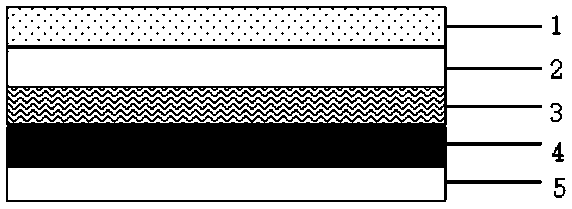
[0046] The film in this embodiment includes a multilayer structure arranged in sequence, and the multilayer structure includes at least a hot-melt adhesive layer with a thickness of 6 μm (note that the hot-melt adhesive layer here is bonded with glass / PC and then peeled off. Force > 20N, low-temperature hot-melt adhesive with working temperature of 75-100°C, boiled in water for 30 minutes without delamination and no whitening); polyether-type TPU substrate layer, its thickness is 100 μm; UV adhesive microstructure coating, of which UV The glue microstructure coating has a surface microstructure, and the microstructure includes wire drawing; the NCVM coating is a tin coating, the thickness of the NCVM coating is 200nm, and an ink layer. The polyurethane used here is polyurethane Costro / Covestro U4299.2wt.%, defoamer BYK011 0.1 wt.%, and wetting agent BYK348 0.7 wt.%.
[0047] The preparation method is as follows:
[0048] Select suitable TPU base material and hot melt adhesive...
Embodiment 2
[0053] The film in this embodiment includes a multilayer structure arranged in sequence, and the multilayer structure includes at least a hot melt adhesive layer with a thickness of 7 μm (note that the hot melt adhesive layer here is bonded with glass / PC and then peeled off. Force > 20N, low-temperature hot-melt adhesive with working temperature of 75-100°C, boiled in water for 30 minutes without delamination and whitening); polyether-type TPU substrate layer, its thickness is 97 μm; UV adhesive microstructure coating, of which UV The glue microstructure coating has a surface microstructure, and the microstructure includes concavo-convex patterns; the NCVM coating is an indium coating, the thickness of the NCVM coating is 300 nm, and an ink layer. The polyurethane used here is polyurethane Costro / Covestro U4299.2wt.%, defoamer BYK011 0.2 wt.%, and wetting agent BYK348 0.6 wt.%.
[0054] The preparation method is as follows:
[0055] Select suitable TPU base material and hot m...
Embodiment 3
[0060] The film in this embodiment includes a multilayer structure arranged in sequence, and the multilayer structure includes at least a hot-melt adhesive layer with a thickness of 6.5 μm (note that the hot-melt adhesive layer here is bonded with glass / PC Peeling force > 20N, low-temperature hot melt adhesive with working temperature of 75-100°C, boiled in water for 30 minutes without delamination and whitening); polyether-type TPU substrate layer, the thickness of which is 95 μm; UV adhesive microstructure coating, of which The UV glue microstructure coating has a surface microstructure, and the microstructure includes a CD pattern; the NCVM coating is an indium coating, the thickness of the NCVM coating is 250nm, and an ink layer. The polyurethane used here is polyurethane Costro / Covestro U4299.4wt.%, defoamer BYK011 0.3 wt.%, and wetting agent BYK348 0.3 wt.%.
[0061] The preparation method is as follows:
[0062] Select suitable TPU base material and hot melt adhesive, ...
PUM
| Property | Measurement | Unit |
|---|---|---|
| thickness | aaaaa | aaaaa |
| thickness | aaaaa | aaaaa |
| thickness | aaaaa | aaaaa |
Abstract
Description
Claims
Application Information


