A Method for Realizing Local Lifetime Control of Semiconductor Devices
A local lifetime control, semiconductor technology, applied in semiconductor/solid-state device manufacturing, electrical components, final product manufacturing, etc. The effect of forward performance and switching performance, process threshold and cost reduction, and on-voltage reduction
- Summary
- Abstract
- Description
- Claims
- Application Information
AI Technical Summary
Problems solved by technology
Method used
Image
Examples
Embodiment 1
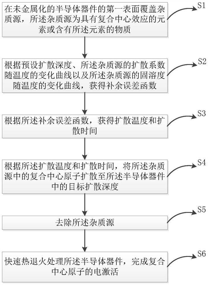
[0041] Embodiment 1 of the present invention provides a method for realizing local lifetime control of semiconductor devices, such as figure 1 shown, including the following steps:
[0042] S1: covering the first surface of the non-metallized semiconductor device with an impurity source, the impurity source being an element having a recombination center effect or a substance containing the element;
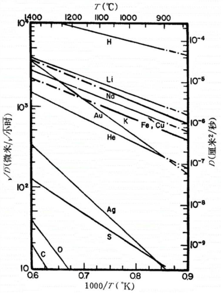
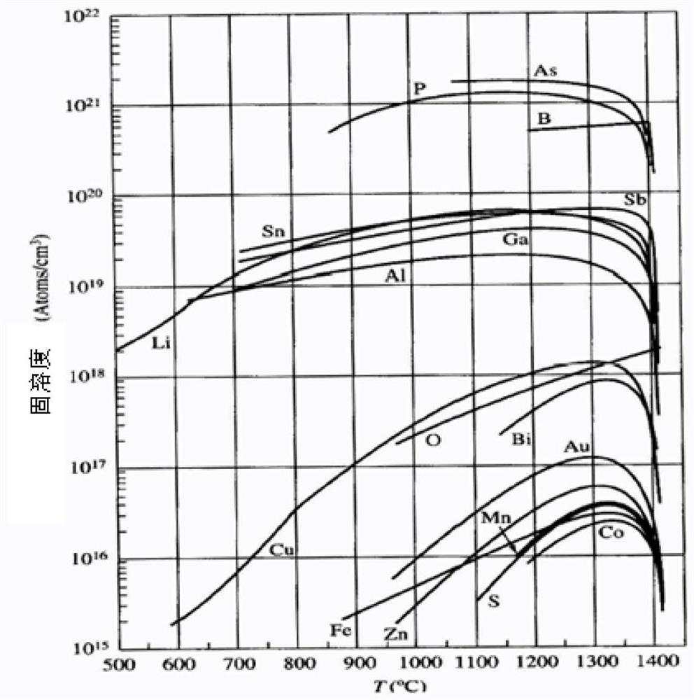
[0043] S2: Obtain the parameters of the complementary error function according to the preset diffusion depth, the variation curve of the diffusion coefficient of the impurity source with temperature, and the variation curve of the solid solubility of the impurity source with temperature;
[0044] S3: Obtain the diffusion temperature and diffusion time according to the parameters of the complementary error function;
[0045] S4: Diffusion the recombination center atoms in the impurity source to a target diffusion depth in the semiconductor device according to the diffusion tempera...
Embodiment 2
[0063] Embodiment 2 of the present invention provides a method for realizing local lifetime control of a semiconductor device, which is based on Embodiment 1 of the present invention, and between step S4 and step S5, further includes step S4(2): removing the impurity source, and then cover the impurity source on the first surface, and repeat steps S2-S4, wherein the preset diffusion depth in step S2 is greater than the preset diffusion depth in step S4(2), thereby forming a second highest life zone 110, the first medium life zone 111, the third low life zone 112, such as Figure 12 As shown, the local lifetime control effect of the step type in the same direction is realized.
Embodiment 3
[0065] Embodiment 3 of the present invention provides a method for realizing local lifespan control of a semiconductor device, which is based on Embodiment 2 of the present invention, and further includes steps between step S4 and step S5:
[0066] S4(1): remove the impurity source, cover the impurity source on a second surface different from the first surface, and repeat steps S2-S4;
[0067] S4(3): remove the impurity source, then cover the impurity source on the second surface, repeat steps S2-S4, wherein the preset diffusion depth in step S4(1) is greater than the preset diffusion depth in step S4(3) Set the diffusion depth.
[0068] According to the above-mentioned embodiment, the third high lifetime region 120, the second medium lifetime region 121, the third medium lifetime region 122, the fourth low lifetime region 123, and the fifth low lifetime region 124 are formed to realize multi-directional and stepped local areas. lifespan control effect.
[0069] In the above...
PUM
| Property | Measurement | Unit |
|---|---|---|
| electrical resistivity | aaaaa | aaaaa |
| thickness | aaaaa | aaaaa |
Abstract
Description
Claims
Application Information


