METHODS for forming semiconductor structures

A semiconductor and bottom electrode technology, applied in the field of formation of semiconductor structures

Inactive Publication Date: 2020-05-08
TAIWAN SEMICON MFG CO LTD
View PDF0 Cites 0 Cited by
  • Summary
  • Abstract
  • Description
  • Claims
  • Application Information

AI Technical Summary

Problems solved by technology

Integrating so many functions on a chip usually presents many new challenges, such as forming and integrating various electronic components and transistor structures

Method used


Image

  • METHODS for forming semiconductor structures
  • METHODS for forming semiconductor structures
  • METHODS for forming semiconductor structures

Examples


Embodiment Construction

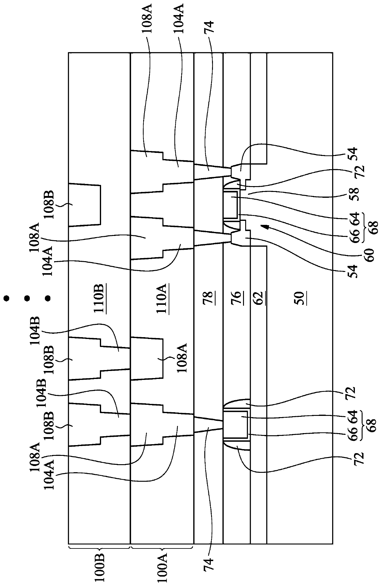
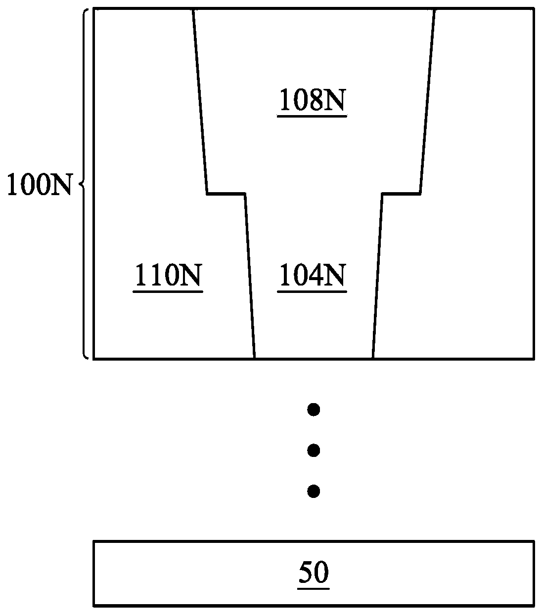
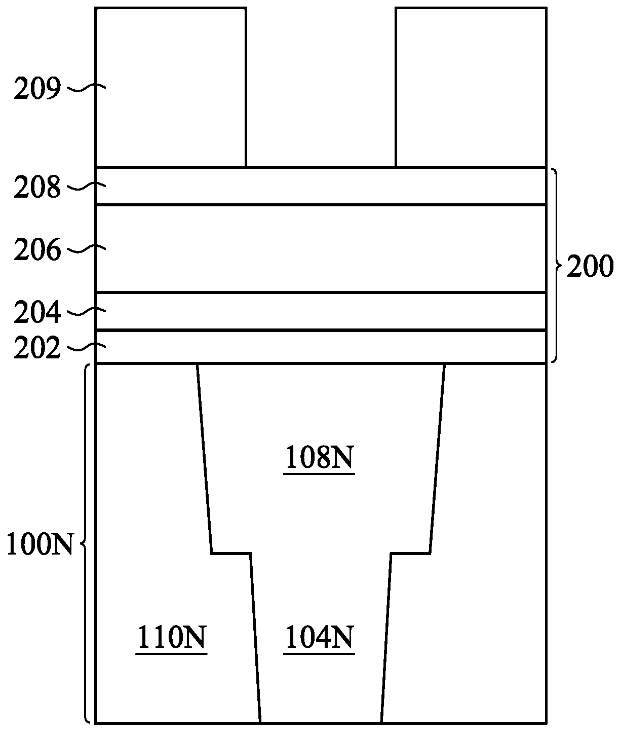
[0053] The following disclosure provides numerous embodiments, or examples, for implementing various elements of the provided subject matter. Specific examples of each element and its configuration are described below to simplify the description of the embodiments of the present invention. Of course, these are just examples, not intended to limit the embodiments of the present invention. For example, if a description mentions that a first element is formed on a second element, it may include an embodiment in which the first and second elements are in direct contact, or may include an additional element formed between the first and second elements , so that they are not in direct contact with the example. In addition, the embodiments of the present invention may repeat reference numerals and / or letters in various examples. This repetition is for the purpose of brevity and clarity and not to show the relationship between the different embodiments and / or configurations discusse...


PUM


Abstract

Methods for forming semiconductor structures and methods of forming magnetic tunnel junction (MTJ) memory cells used in a magneto-resistive random access memory (MRAM) array are provided. A pre-cleanprocess is performed to remove a metal oxide layer that may form on the top surface of the bottom electrodes of MTJ memory cells during the time the bottom electrode can be exposed to air prior to depositing MTJ layers. The pre-clean processes may include a remote plasma process wherein the metal oxide reacts with hydrogen radicals generated in the remote plasma.

Description

technical field [0001] Embodiments of the present invention relate to a method for forming a semiconductor structure, in particular to a method for forming a magnetoresistive random access memory. Background technique [0002] The semiconductor industry continues to increase the density of electronic components (such as transistors, diodes, resistors, capacitors, etc.) in integrated circuits through the innovation of semiconductor technology. Such innovations include progressive reductions in minimum feature size; three-dimensional transistor structures (such as fin field-effect transistors (FinFETs)); increased number of interconnection layers; and interconnections stacked on top of semiconductor substrates. Non-semiconductor memories in the layer, such as ferroelectric random access memory (FRAM) and magnetoresistive random access memory (magneto-resistive RAM, MRAM). The basic storage element of the MRRAM is a magnetic tunnel junction (MTJ). High component density enabl...

Claims


Application Information

Patent Timeline
Patent Type & Authority Applications(China)
IPC IPC(8): H01L27/22H01L43/08H01L43/10H01L43/12
CPCH10B61/22H10N50/01H10N50/85H10N50/10H10N50/80
Inventor 吴荣堂吴孟谕吴思桦李锦思
Owner TAIWAN SEMICON MFG CO LTD
Why Eureka
Try Eureka