Silicon carbide semi-accumulation type channel MOSFET device and preparation method thereof

A trench device and accumulation technology, which is applied in semiconductor/solid-state device manufacturing, semiconductor devices, electrical components, etc., can solve the problem that trench gate oxide is easy to be broken down

Pending Publication Date: 2020-05-08
SOUTH UNIVERSITY OF SCIENCE AND TECHNOLOGY OF CHINA
View PDF6 Cites 1 Cited by
  • Summary
  • Abstract
  • Description
  • Claims
  • Application Information

AI Technical Summary

Problems solved by technology

However, trench MOSFET devices face the disadvantage that the trench gate oxide is easily broken down in the blocking state, and an additional protective structure is usually required to shield the gate oxide.

Method used


Image

  • Silicon carbide semi-accumulation type channel MOSFET device and preparation method thereof
  • Silicon carbide semi-accumulation type channel MOSFET device and preparation method thereof
  • Silicon carbide semi-accumulation type channel MOSFET device and preparation method thereof

Examples


Embodiment

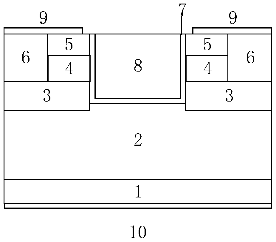
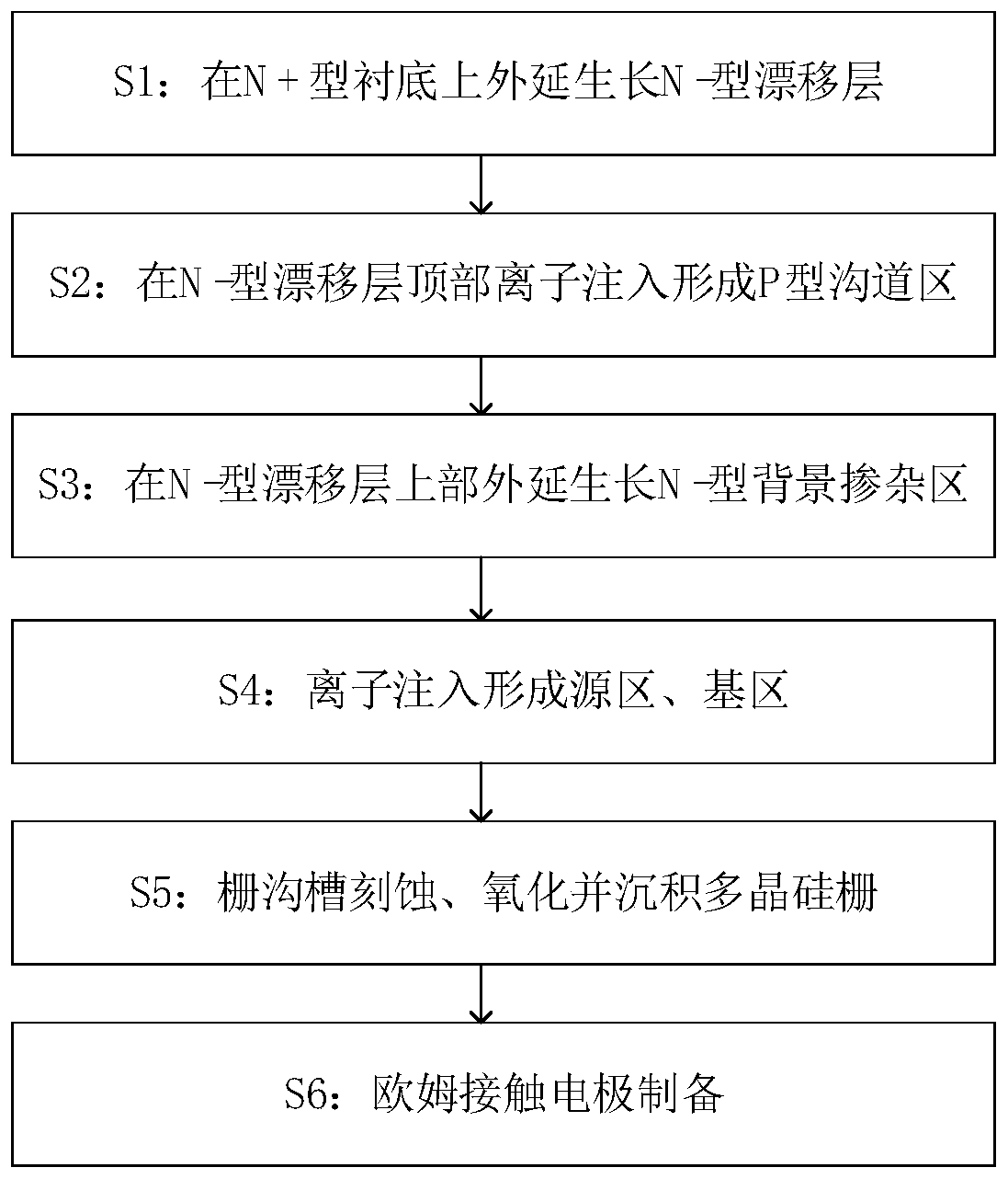
[0051] An embodiment of the present invention provides a silicon carbide semi-accumulation channel MOSFET device, the device structure is as follows figure 1 As shown, the structure includes an N+ type substrate 1 with an N− type epitaxial drift region 2 on top of it. On top of the N-type epitaxial drift region 2, there is a P-type channel region 3. The top of the N-type epitaxial drift region 2 is the N-type background doped region 4, and the source region 5 and the base region 6 are formed by ion implantation, wherein the depth of the base region 6 is relatively deep, and its bottom is deep into the P-type channel region 3 among. The center of the top of the device structure is a trench structure, the sidewall of the trench is covered with a gate oxide layer 7 , and the inside of the trench is filled with a gate electrode 8 .

[0052] The doping concentration of the P-type channel region 3 is 3×10 17 cm -3 , the vertical height (along the device axial direction) is 0.5 μ...


PUM

PropertyMeasurementUnit
heightaaaaaaaaaa
thicknessaaaaaaaaaa
thicknessaaaaaaaaaa

Abstract

The invention provides a silicon carbide semi-accumulation type channel device. A silicon carbide semi-accumulation type channel MOSFET device has the characteristics of high channel carrier mobilityand high threshold voltage. The structure comprises an N+ type substrate, and an N-type epitaxial drift region is arranged at the upper part of the N+ type substrate. And a P-type channel region is arranged at the top of the N-type epitaxial drift region. An N-type background doped region is arranged above the N-type epitaxial drift region, a source region and a base region are formed through ionimplantation, the depth of the base region is large, and the bottom of the base region goes deep into the P-type channel region. The center of the top of the device structure is a groove structure, aside wall of a groove is covered with a gate oxide layer, and the groove is filled with a gate electrode. The total channel length of the device is 0.6-1 micrometer, the length of an inversion channel, adjacent to the gate oxide layer, of the P-type channel region is 0.1-0.2 micrometer, and the remaining channel part is an accumulation channel. The invention also provides a preparation method of the silicon carbide semi-accumulation type channel device.

Description

technical field [0001] The invention belongs to the technical field of semiconductor power devices, and in particular relates to a silicon carbide semi-accumulated channel device and a preparation method. Background technique [0002] Silicon carbide material has excellent material properties and is considered to be the core material of next-generation power semiconductor technology. At present, silicon carbide power semiconductor devices have been widely used in new energy vehicles, solar energy, wind power generation and many other fields. Silicon carbide MOSFET devices have the advantages of high input impedance and easy driving, and are currently the most concerned silicon carbide power semiconductor devices. However, SiC MOSFETs suffer from high channel resistance due to lower channel carrier mobility. [0003] The carrier mobility of SiC channel is restricted by scattering, and the main scattering mechanisms are surface roughness scattering and Coulomb scattering. Am...

Claims


Application Information

Patent Timeline
Patent Type & Authority Applications(China)
IPC IPC(8): H01L29/78H01L21/336H01L29/10H01L29/16
CPCH01L29/78H01L29/66477H01L29/1025H01L29/1608
Inventor 温正欣张新河杨安丽陈施施叶怀宇张国旗
Owner SOUTH UNIVERSITY OF SCIENCE AND TECHNOLOGY OF CHINA
Why Eureka
Try Eureka