Chamber washing device and method and semiconductor processing equipment

A technology for cleaning devices and chambers, which is used in gaseous chemical plating, metal material coating processes, coatings, etc., and can solve the problem of frequent use of plasma sources and other issues

Active Publication Date: 2020-05-15
BEIJING NAURA MICROELECTRONICS EQUIP CO LTD
View PDF5 Cites 5 Cited by
  • Summary
  • Abstract
  • Description
  • Claims
  • Application Information

AI Technical Summary

Problems solved by technology

The plasma source is frequently used, so how to ensure the stability and consistency of the PEALD process results bef...

Method used


Image

  • Chamber washing device and method and semiconductor processing equipment
  • Chamber washing device and method and semiconductor processing equipment
  • Chamber washing device and method and semiconductor processing equipment

Examples


Embodiment Construction

[0027] Specific embodiments of the present invention will be described in detail below in conjunction with the accompanying drawings. It should be understood that the specific embodiments described here are only used to illustrate and explain the present invention, and are not intended to limit the present invention.

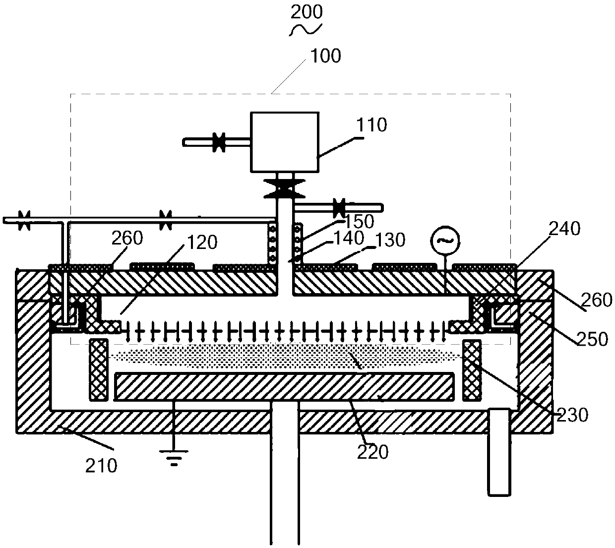
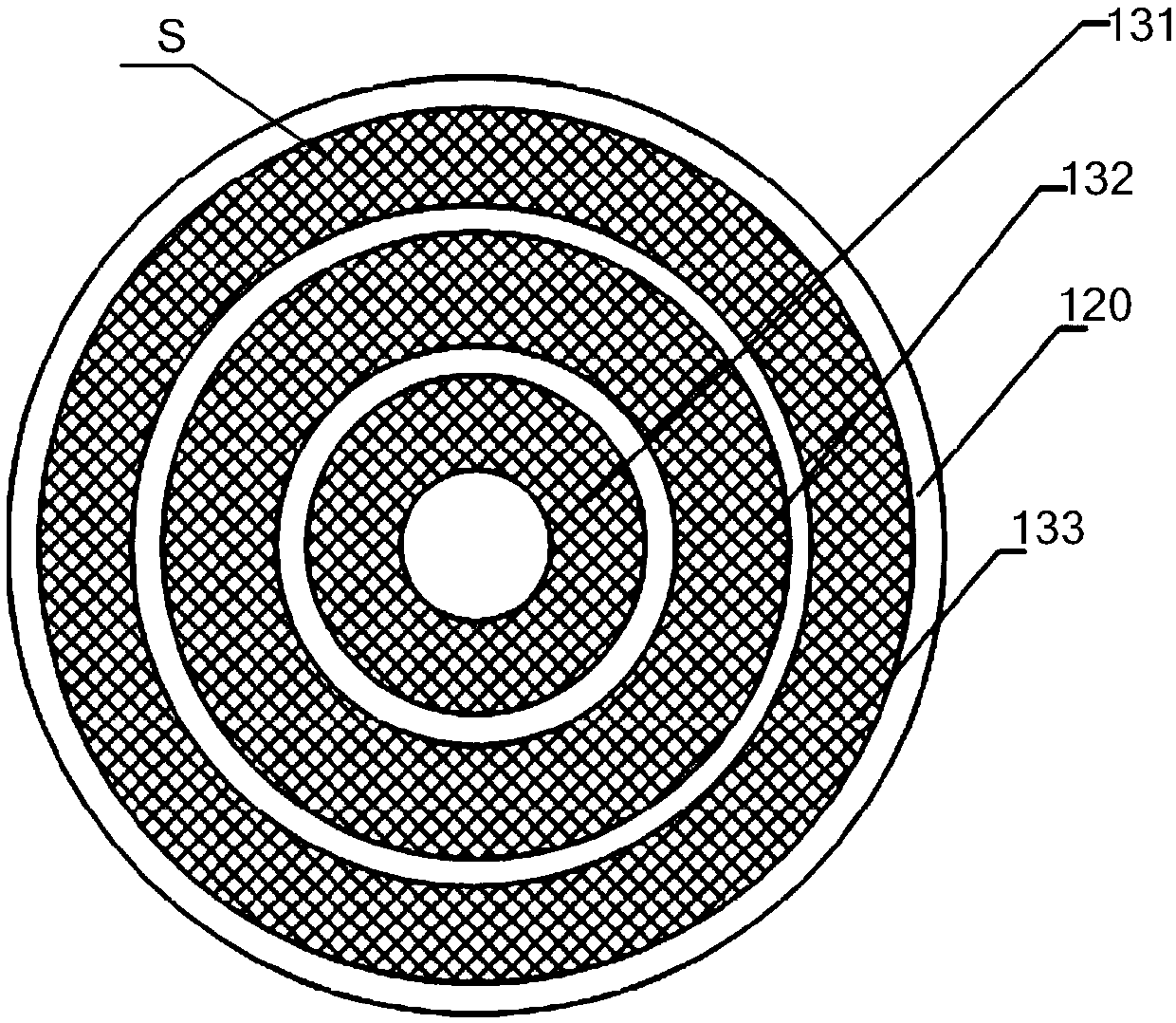
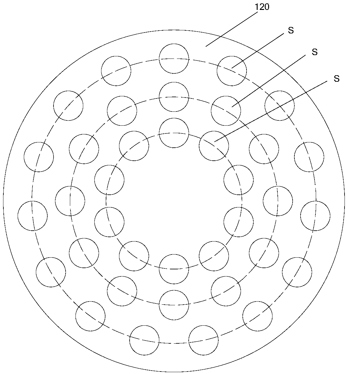
[0028] like figure 1 As shown, the first aspect of the present invention relates to a chamber cleaning device 100, the cleaning device 100 may include a cleaning plasma source 110 and a flow equalizer 120 connected to the cleaning plasma source 110, for example, cleaning plasma Source 110 may be connected to flow divider 120 via cleaning plasma source delivery line 140 as described below. The cleaning plasma source 110, for example, may be a remote plasma source (Remote Plasma Source, RPS), or may also be other structures capable of exciting cleaning gas to generate cleaning plasma. A number of uniform flow holes are generally arranged on the flow uniform memb...


PUM


Abstract

The invention discloses a chamber washing device and method and semiconductor processing equipment. The chamber washing device comprises a washing plasma source and a uniform flow piece connected withthe washing plasma source, wherein a heating strip is arranged on the uniform flow piece and forms a plurality of concentric ring structures on the surface of the uniform flow piece; and the heatingpower of the concentric ring structures can be adjusted to selectively enable the uniform flow piece to have a plurality of different temperature zones, so that after the washing technology is finished, the temperature at each part of the uniform flow piece is ensured to rapidly recover to the set temperature, the temperature uniformity can rapidly meet the requirement, the cooling time after finishing the washing technology can be further shortened, and the deposition rate and the film uniformity during the following deposition technology are improved.

Description

technical field [0001] The invention relates to the technical field of semiconductor manufacturing, in particular to a chamber cleaning device, a chamber cleaning method and semiconductor processing equipment. Background technique [0002] In the semiconductor industry, as the geometries of electronic devices continue to shrink and the density of devices continues to increase, feature size and aspect ratio become more and more challenging. Atomic Layer Deposition (ALD) is a new thin film deposition method proposed to meet this challenge. With its unique self-limiting growth mode, atomic layer deposition has the advantages of precise and controllable film growth thickness, excellent shape retention, and controllable composition. It has attracted more and more attention from scientific and technological workers all over the world. [0003] The heat-induced ALD process, the most common ALD technique, uses heat to create a chemical reaction between two reactants. Although ther...

Claims


Application Information

Patent Timeline
IPC IPC(8): C23C16/44C23C16/455C23C16/513
CPCC23C16/4405C23C16/45544C23C16/513
Inventor 丁安邦史小平陈鹏兰云峰
Owner BEIJING NAURA MICROELECTRONICS EQUIP CO LTD
Why Eureka
Try Eureka