Check patentability & draft patents in minutes with Patsnap Eureka AI!

Array substrate unit and preparation method thereof, array substrate and display control system

An array substrate and display control technology, applied in nonlinear optics, instruments, optics, etc., can solve the problems of dead pixels, high price, and difficult manufacturing process, and achieve the effect of simple manufacturing process, simple structure, and low cost

Inactive Publication Date: 2020-05-15
FUJIAN INST OF RES ON THE STRUCTURE OF MATTER CHINESE ACAD OF SCI
View PDF6 Cites 0 Cited by
  • Summary
  • Abstract
  • Description
  • Claims
  • Application Information

AI Technical Summary

Problems solved by technology

[0003] In the related technology, DMD devices arrange a matrix composed of microlenses on a semiconductor chip. Under the control of digital drive signals, these microlenses absorb unnecessary light through light absorbers to realize image projection. However, the quality of DMD chips The requirements are very high, the preparation process is difficult, and the controller of the DMD chip is a consumable, the price is high, and it is easy to cause dead pixels. Once damaged, it is easy to cause the entire projection instrument to be unusable. Therefore, it is necessary to propose an alternative to DMD. device display device

Method used


Image

  • Array substrate unit and preparation method thereof, array substrate and display control system
  • Array substrate unit and preparation method thereof, array substrate and display control system
  • Array substrate unit and preparation method thereof, array substrate and display control system

Examples


preparation example Construction

[0077] The embodiment of the present application also provides a method for preparing an array substrate unit, including:

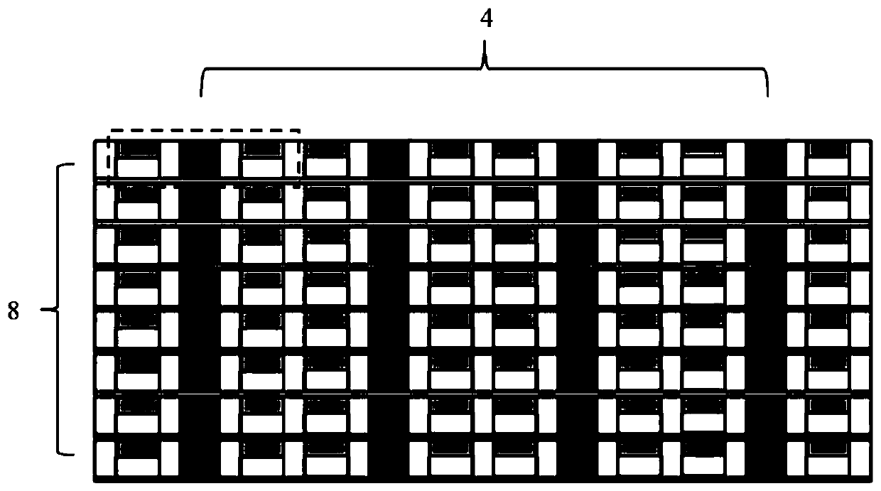
[0078] First, a waveguide layer is formed on a substrate.

[0079] Optionally, the substrate is selected from inorganic materials such as lithium niobate, lithium tantalate, lithium niobate doped with magnesium oxide, silicon dioxide, tantalum pentoxide, niobium pentoxide, etc.; organic materials such as plastics, plexiglass, etc.; semiconductor materials Any one of CaAs, GaAsP, InGaAlP, etc.

[0080] Optionally, the preparation process of the waveguide layer includes: firstly, providing a waveguide base layer; secondly, forming a substrate medium layer covering the waveguide base layer and a light-guiding medium layer covering the substrate medium layer; finally, performing a process on the light-guiding medium layer Patterning process to obtain the waveguide layer. Among them, the waveguide base layer is selected from base materials such as lithium ni...


PUM


Abstract

The invention discloses an array substrate unit and a preparation method thereof, an array substrate and a display control system. The array substrate unit comprises a substrate; a waveguide layer, arranged on the substrate; an electrode layer pair, arranged on the substrate, and the waveguide layer being located between the electrode layer pair; and a control circuit, connected with the electrodelayer pairs and used for controlling a voltage value between the electrode layer pairs so as to change an optical path in the waveguide layer between the electrode layer pairs. According to the arraysubstrate unit, the voltage value between the electrode layer pairs can be changed through the control circuit, and the light path in the waveguide layer between the electrode layer pairs is adjusted, so that the array substrate unit has different display results under different voltage values.

Description

technical field [0001] The present application relates to the field of display technology, in particular, to an array substrate unit and a manufacturing method thereof, an array substrate, and a display control system. Background technique [0002] At present, in the field of projection display technology, LCOS (Liquid Crystal on Silicon) reflective projection display technology and DLP (Digital Light Processing, digital optical processing technology) are widely used due to their high brightness and high definition. Among them, the DLP imaging technology digitally processes the image signal and then projects the light to generate an image. This process requires the core component DMD (Digital Micromirror Device, digital micromirror device) to complete the visual digital optical processing. process. [0003] In the related technology, DMD devices arrange a matrix composed of microlenses on a semiconductor chip. Under the control of digital drive signals, these microlenses ab...

Claims


Application Information

Patent Timeline
IPC IPC(8): G02F1/03G02F1/035
CPCG02F1/0305G02F1/0316G02F1/0327G02F1/035
Inventor 冯新凯陈怀熹李广伟张新彬古克义梁万国
Owner FUJIAN INST OF RES ON THE STRUCTURE OF MATTER CHINESE ACAD OF SCI
Features
  • R&D
  • Intellectual Property
  • Life Sciences
  • Materials
  • Tech Scout
  • Unparalleled Data Quality
  • Higher Quality Content
  • 60% Fewer Hallucinations
Learn More