Ion implantation method and ion implantation system

An ion implantation system and ion implantation technology, applied in the field of ion implantation methods and ion implantation systems, can solve problems affecting the electrical properties and yield of devices, and achieve the elimination of the impact caused by ion implantation effects, uniform electrical properties, and better uniformity electrical effect

Active Publication Date: 2020-05-15
YANGTZE MEMORY TECH CO LTD
View PDF5 Cites 2 Cited by
  • Summary
  • Abstract
  • Description
  • Claims
  • Application Information

AI Technical Summary

Problems solved by technology

[0004] In view of the above-mentioned shortcomings of the prior art, the object of the present invention is to provide an ion implantation method and an ion implantation system, which are used to solve the problem in the prior art that the channel holes in the edge region of the wafer are relatively vertical to the wafer surface. The ion implantation at the bottom of the channel via hole in different regions of the wafer is very different due to the inclination of the direction of the ion implantation process at a certain angle, which affects the electrical properties and yield of the device.

Method used


Image

  • Ion implantation method and ion implantation system
  • Ion implantation method and ion implantation system
  • Ion implantation method and ion implantation system

Examples


Embodiment 1

[0041] see figure 1 , the present embodiment also provides an ion implantation method, the ion implantation method includes the following steps:

[0042] 1) A wafer is provided, and several channel holes are formed in the wafer, and the communication holes located in the central area of ​​the wafer are perpendicular to the surface of the wafer, and the channels located in the edge area of ​​the wafer the holes are inclined at an angle of less than 90° relative to a direction perpendicular to the wafer surface; and

[0043] 2) making the wafer reciprocate in an arc along a first direction, and perform ion implantation into the wafer along a second direction, the first direction being perpendicular to the second direction.

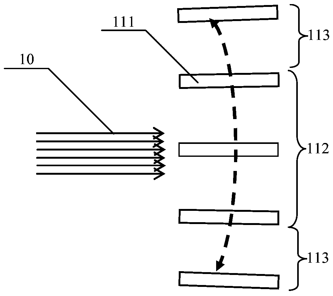
[0044] In step 1), see figure 1 Step S1 in and figure 2 , a wafer is provided, and several channel holes 111 are formed in the wafer, and the communication holes 111 located in the central region 112 of the wafer are perpendicular to the surface of the w...

Embodiment 2

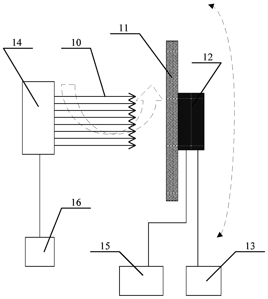
[0065] Please combine Figure 1 to Figure 2 refer to image 3 , an ion implantation system is also provided in this embodiment, and the ion implantation system includes: a wafer chuck 12, the wafer chuck 12 is used to absorb the wafer 11, and several channels are formed in the wafer 11 hole 111, and the communication hole 111 located in the wafer center area 112 is perpendicular to the surface of the wafer 11, and the channel hole 111 located in the wafer edge area 113 is compared to the channel hole 111 perpendicular to the wafer 11 The direction of the surface is inclined at an angle less than 90°; the first driving device 13, the first driving device 13 is connected with the wafer chuck 12, and the first driving device is used to drive the wafer chuck 12 to drive the wafer chuck 12 The wafer 11 performs an arc-shaped reciprocating movement along a first direction; and an ion implantation device 14, the ion implantation device 13 performs ion implantation into the wafer 11 ...


PUM


Abstract

The invention provides an ion implantation method and an ion implantation system. The ion implantation method comprises the following steps of providing a wafer, wherein a plurality of channel holes are formed in the wafer, the communication holes located in the center area of the wafer are perpendicular to the surface of the wafer, and the channel holes located in the edge area of the wafer incline by an angle smaller than 90 degrees relative to the direction perpendicular to the surface of the wafer; and enabling the wafer to perform arc reciprocating motion along a first direction, and carrying out ion implantation in the wafer along a second direction, wherein the first direction is perpendicular to the second direction. According to the ion implantation method provided by the invention, in the process of carrying out ion implantation along the second direction to enable the wafer to do arc-shaped reciprocating motion along the first direction vertical to the second direction, theions can be ensured to be injected into the bottom of each channel hole, so that the ion implantation quantities of the bottoms of the channel holes are the same, the influence of different inclination degrees of the channel holes in different regions of the wafer relative to the direction perpendicular to the surface of the wafer on the ion implantation effect is eliminated, the electrical property and yield of a device can be ensured, and the whole wafer has better and more uniform electrical property.

Description

technical field [0001] The invention belongs to the technical field of integrated circuits, and in particular relates to an ion implantation method and an ion implantation system. Background technique [0002] In the 3D NAND production process, affected by the Etch (etching) process, the channel holes (Channel Hole, CH) in the center of the wafer (Wafer Center) and the edge of the wafer (Wafer Edge) are compared with those on the surface of the wafer. Tilting performance (TitlingPerformance) is not the same, for example, the trench hole at the center of the wafer is perpendicular to the wafer surface, while the trench hole at the edge of the wafer is perpendicular to the wafer surface The direction of the channel hole is inclined at a certain angle, and the closer to the edge of the wafer, the more serious the inclination of the channel hole is. [0003] In the existing ion implantation process, the ion beam is generally implanted in a direction perpendicular to the surface...

Claims


Application Information

Patent Timeline
Patent Type & Authority Applications(China)
IPC IPC(8): H01L21/265H01L21/67
CPCH01L21/26506H01L21/67011
Inventor 艾义明
Owner YANGTZE MEMORY TECH CO LTD
Why Eureka
Try Eureka