LTPS TFT Substrate Structure and Method of Forming the Same

a thin film transistor and substrate technology, applied in the field of display technology, can solve the problems of poor uniformity in the display area and affect the quality of ltps tft substrates, and achieve the effects of improving uniformity, reducing laser energy, and reducing the number of electrons

Active Publication Date: 2016-06-30
TCL CHINA STAR OPTOELECTRONICS TECH CO LTD
View PDF2 Cites 1 Cited by
  • Summary
  • Abstract
  • Description
  • Claims
  • Application Information

AI Technical Summary

Benefits of technology

[0018]An object of the present invention is to provide a method of forming a LTPS TFT substrate that has relatively larger poly-Si dies and attains to higher electron mobility in the drive area, so to elevate the electrical characteristics of the driver. On the other hand, it has relatively smaller poly-Si dies with better uniformity in the display area, so that the electrical property of the TFT within the display area can be more even, and the quality of the LTPS TFT substrate is improved.
[0019]Another object of the present invention is to provide a LTPS TFT substrate structure with its poly-Si region in the drive area producing larger poly-Si dies and poly-Si region in the display area producing smaller poly-Si dies with better uniformity. Thus the drive has better electrical characteristics, and the TFT in the display area has more uniformed electrical property, so that the TFT substrate will have higher quality.
[0047]The present invention brings several benefits. The forming method of the LTPS TFT substrate of the present invention first deposits and patterns a layer of silicon oxide on the a-Si layer, producing a layer of silicon oxide on the a-Si layer in the display area. Then, the silicon oxide layer serves as a photomask when the a-Si layer is annealed by excimer laser and crystalizes, and turns into a poly-Si layer. It forms relatively larger dies in the drive area and attains to higher electron mobility. The display area, because of the shielding of the silicon oxide layer, is exposed to lower laser energy, thus forms relatively smaller dies with better uniformity. It ensures a more even electron mobility in the display area and enhances the quality of the LTPS TFT substrate. The forming process is simple and easy to operate. In addition, the present invention provides a LTPS TFT substrate structure with poly-Si regions in the drive area producing larger dies than in the display area, so to ensure that the drive has better electrical characteristics and the TFT within the display area has more even electrical property. The TFT substrate, therefore, has better quality.

Problems solved by technology

The conventional forming method of the LTPS TFTs results in poorer uniformity in the display area, and lower-than-expected electron mobility of the driver in the drive area, further affecting the quality of LTPS TFT substrates.

Method used


Image

  • LTPS TFT Substrate Structure and Method of Forming the Same
  • LTPS TFT Substrate Structure and Method of Forming the Same
  • LTPS TFT Substrate Structure and Method of Forming the Same

Examples


Embodiment Construction

[0061]The drawings illustrate embodiments of the invention and, together with the description, serve to explain the principles of the invention.

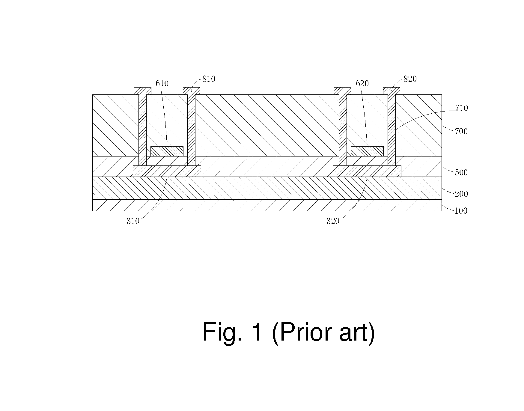
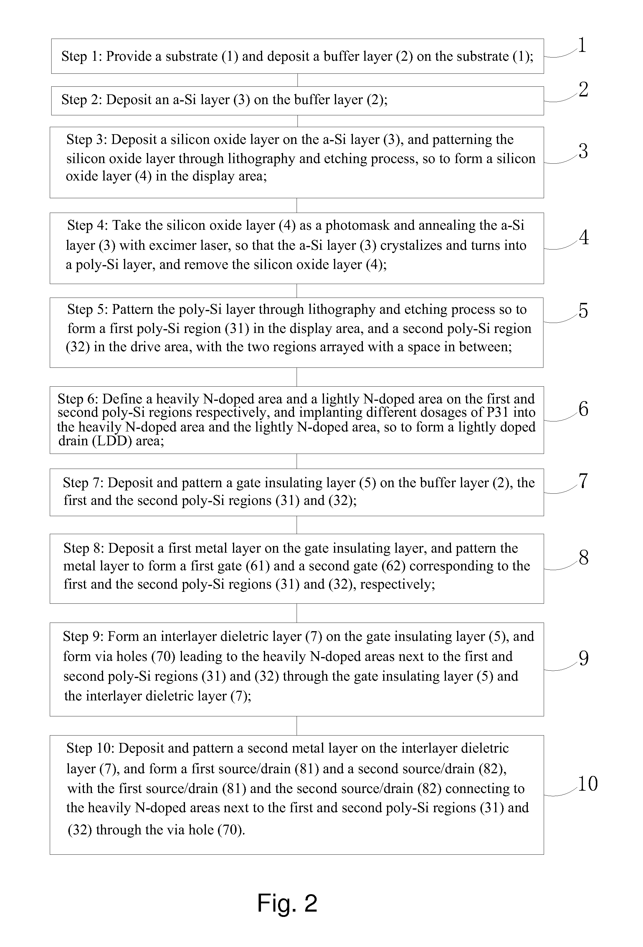
[0062]Please refer to FIG. 1. The present invention provides a method of forming a LTPS TFT substrate comprising the following steps:

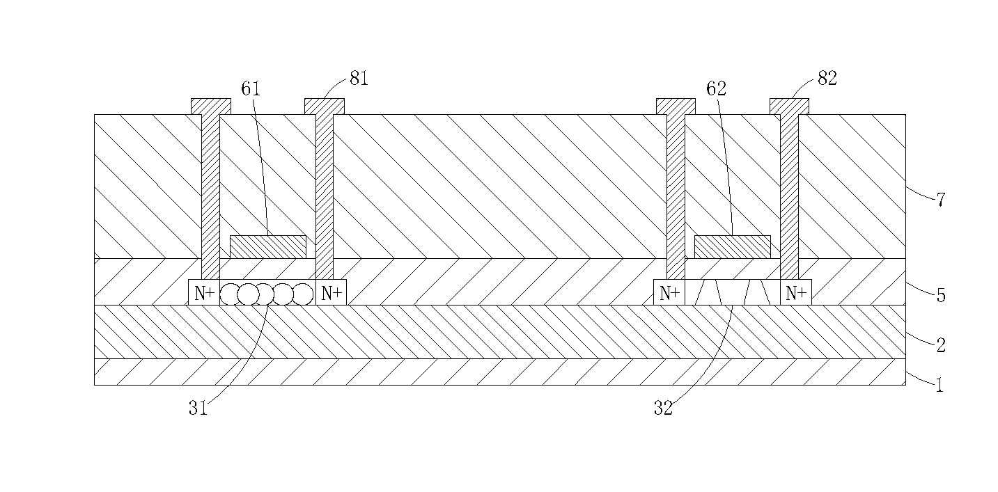
[0063]Step 1: Provide a substrate 1, and deposit a buffer layer 2 on the substrate 1, as shown in FIG. 3.

[0064]The substrate 1 is a transparent substrate which is made, preferably, of glass or plastic.

[0065]Specifically, the materials of the buffer layer 2 can be either silicon nitride (SiNx), silicon oxide (SiOx), or the combination of the two.

[0066]Step 2: Deposit an a-Si layer 3 on the buffer layer 2, as shown in FIG. 4.

[0067]Step 3: As shown in FIG. 5, deposit a silicon oxide layer on the a-Si layer 3, and pattern the silicon oxide layer through lithography and etching process so to get a silicon oxide layer 4 in the display area. The a-Si layer 3 in the drive area of the non-display area, at this stage, is...


PUM

PropertyMeasurementUnit
brightnessaaaaaaaaaa
electron mobilityaaaaaaaaaa
flexibilityaaaaaaaaaa

Abstract

A method of forming an LTPS TFT substrate includes: Step 1: providing a substrate (1) and depositing a buffer layer (2); Step 2: depositing an a-Si layer (3); Step 3: depositing and patterning a silicon oxide layer (4); Step 4: taking the silicon oxide layer (4) as a photomask and annealing the a-Si layer (3) with excimer laser, so that the a-Si layer crystalizes and turns into a poly-Si layer; Step 5: forming a first poly-Si region (31) and a second poly-Si region (32); Step 6: defining a heavily N-doped area and a lightly N-doped area on the first and second poly-Si regions (31) and (32), and forming an LDD area; Step 7: depositing and patterning a gate insulating layer (5); Step 8: forming a first gate (61) and a second gate (62); Step 9: forming via holes (70); and Step 10: forming a first source / drain (81) and a second source / drain (82).

Description

BACKGROUND OF THE INVENTION[0001]1. Field of the Invention[0002]The present invention relates to display technology, and more specifically, to a low temperature poly-silicon (LTPS) thin-film transistor (TFT) substrate structure and a method of forming the same.[0003]2. Description of the Prior Art[0004]Thin-film transistor liquid crystal display (TFT-LCD) can be achieved by two approaches: polycrystalline silicon (poly-Si) and amorphous silicon (a-Si). Low temperature poly-silicon (LTPS) is the latest generation of TFT-LCD producing technology. The biggest different between a LTPS TFT-LCD and a conventional a-Si TFT-LCD is that the former responds faster, has higher brightness and resolution, and consumes less power.[0005]The crystalline silicons used by LTPS technology are arrayed more orderly than that used by a-Si technology. Therefore, the electron mobility of LTPS technology is over 100 times higher than that of a-Si technology. The peripheral driver can be built on the same gl...

Claims


Application Information

Patent Timeline
Patent Type & Authority Applications(United States)
IPC IPC(8): H01L27/12H01L29/08H01L21/283H01L29/04H01L29/16H01L21/31H01L21/311H01L21/324H01L21/306H01L21/223H01L21/3213H01L21/768H01L29/49H01L29/786H01L23/522H01L29/66
CPCH01L27/1218H01L27/124H01L29/0847H01L21/283H01L29/04H01L29/16H01L21/31H01L21/31144H01L21/324H01L21/30604H01L21/223H01L21/32133H01L21/76802H01L21/76877H01L29/4908H01L29/495H01L29/4958H01L29/78675H01L23/5226H01L27/1222H01L29/66757H01L27/1214H01L27/1259H01L2924/0002H01L27/1285H01L27/1229H01L27/127H01L27/1288H01L29/78621H01L2924/00H01L21/02532H01L21/02592H01L21/02678H01L21/0332H01L21/0335H01L21/0337H01L21/26513H01L21/3065H01L27/1274H01L29/66598
Inventor LU, GAIPING
Owner TCL CHINA STAR OPTOELECTRONICS TECH CO LTD
Why Eureka
Try Eureka