Polishing equipment for semiconductor wafer production

A semiconductor and wafer technology, applied in the field of semiconductor processing equipment, can solve the problems of easy sliding of semiconductor materials, complex equipment structure, and high cost of polishing heads

Active Publication Date: 2020-05-19
北京博文合锋咨询有限公司
View PDF5 Cites 2 Cited by
  • Summary
  • Abstract
  • Description
  • Claims
  • Application Information

AI Technical Summary

Problems solved by technology

[0004] Aiming at the deficiencies in the prior art, the purpose of the present invention is to provide a polishing device for semiconductor wafer production, to solve the problem that the existing fixing methods are mostly nesting methods when polishing, and the semico

Method used


Image

  • Polishing equipment for semiconductor wafer production
  • Polishing equipment for semiconductor wafer production
  • Polishing equipment for semiconductor wafer production

Examples


no. 1 example

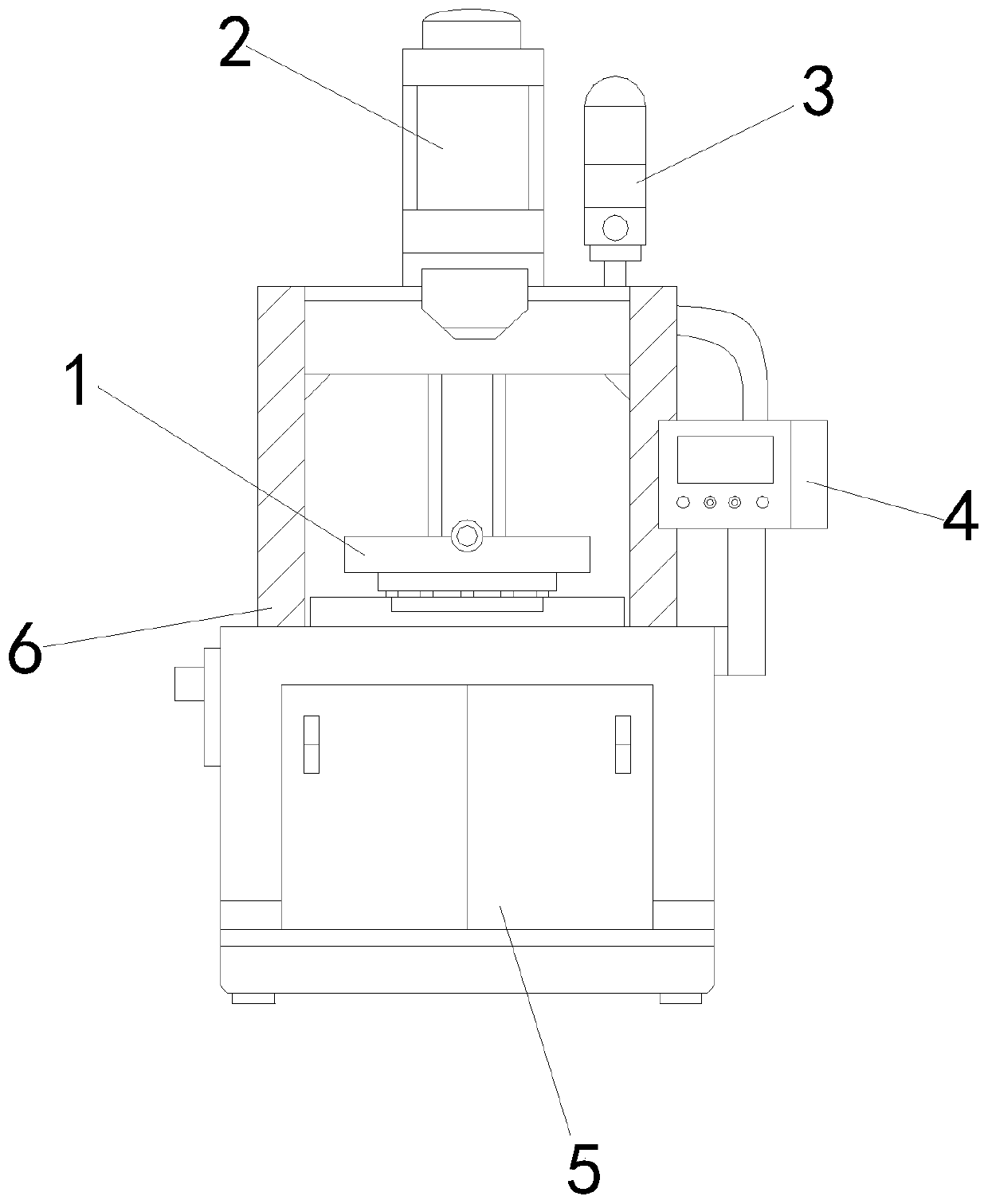
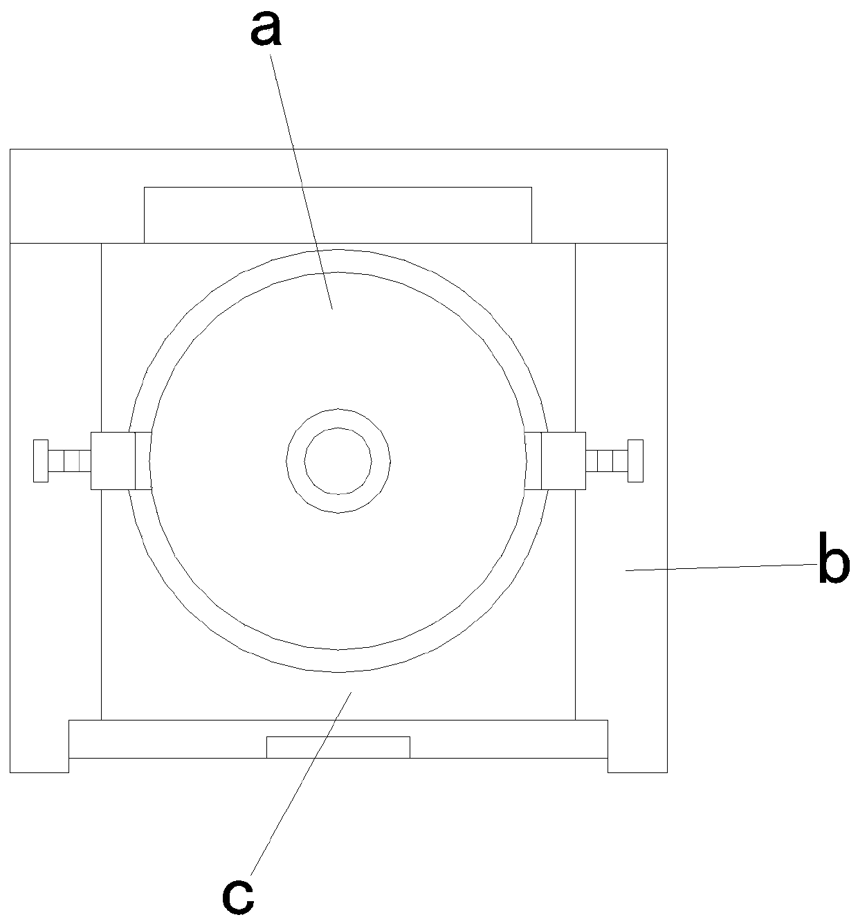
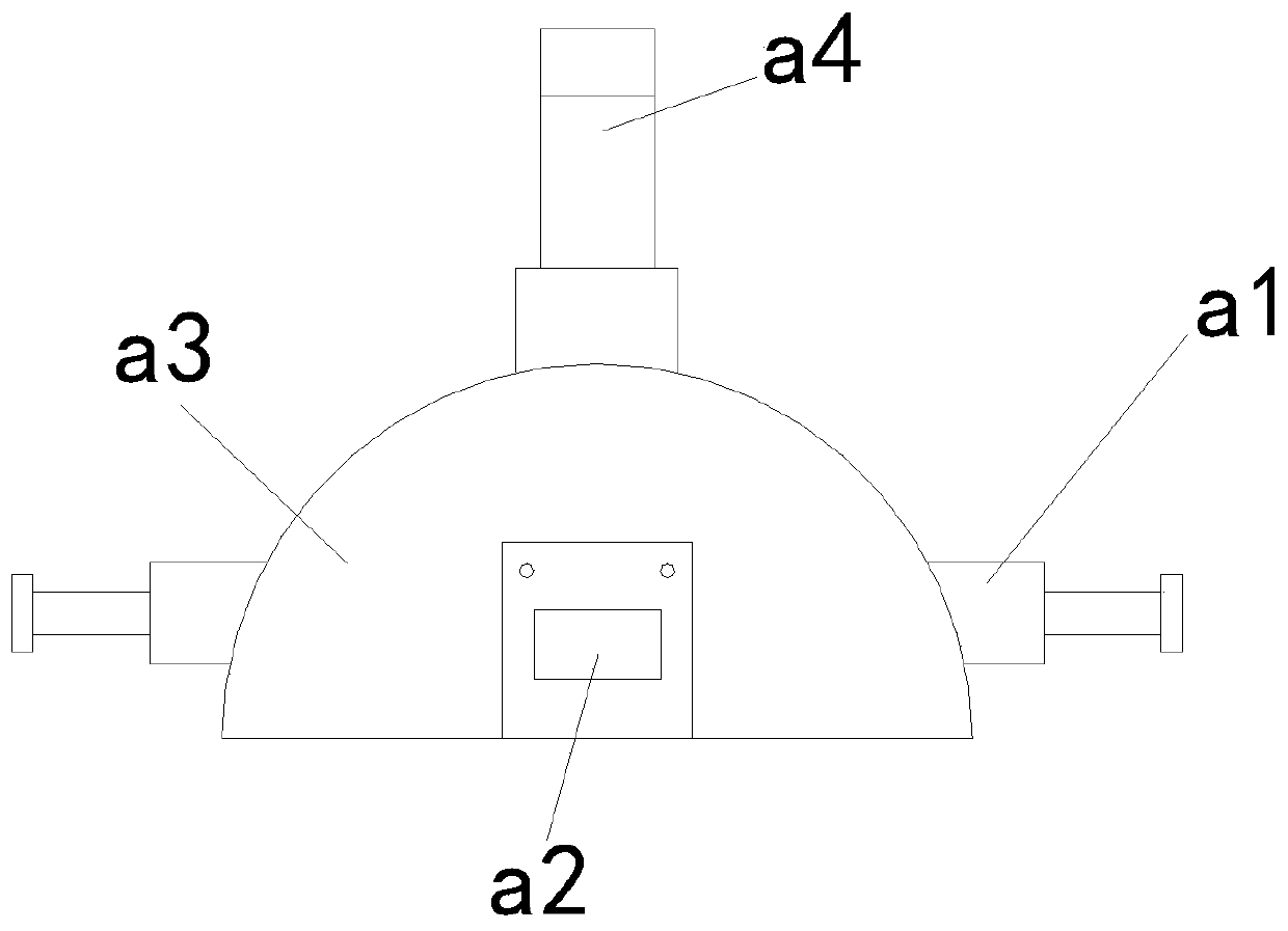
[0026] see Figure 5-Figure 6 , the present invention provides a technical scheme of polishing equipment for semiconductor wafer production: its structure includes: a polishing equipment for semiconductor wafer production, its structure includes: processing head body 1, power device 2, indicator light 3 , a controller 4, a bearing box 5, and an outer frame 6. The processing head body 1 is installed below the power device 2 and is fastened with the power device 2. The power device 2 is arranged on the upper end of the outer frame 6, and the outer frame 6 Locked with the power unit 2, a bearing box 5 is provided below the outer frame 6, the bearing box 5 is locked with the outer frame 6, a controller 4 is arranged on the side of the outer frame 6, and a controller 4 is arranged above the controller 4 An indicator light 3 is provided, and the indicator light 3 is electrically connected to the controller 4. The processing head body 1 includes a polishing buckle device a, an assemb...

no. 2 example

[0031] see Figure 1-Figure 4, the present invention provides a technical scheme of polishing equipment for semiconductor wafer production: its structure includes: a polishing equipment for semiconductor wafer production, its structure includes: processing head body 1, power device 2, indicator light 3 , a controller 4, a bearing box 5, and an outer frame 6. The processing head body 1 is installed below the power device 2 and is fastened with the power device 2. The power device 2 is arranged on the upper end of the outer frame 6, and the outer frame 6 Locked with the power unit 2, a bearing box 5 is provided below the outer frame 6, the bearing box 5 is locked with the outer frame 6, a controller 4 is arranged on the side of the outer frame 6, and a controller 4 is arranged above the controller 4 An indicator light 3 is provided, and the indicator light 3 is electrically connected to the controller 4. The processing head body 1 includes a polishing buckle device a, an assembl...


PUM


Abstract

The invention discloses polishing equipment for semiconductor wafer production. The polishing equipment structurally comprises a machining head machine body, a power device, an indicator lamp, a controller, a bearing box and an outer frame; the machining head machine body is installed on the lower portion of the power device and is in fastening with the power device; the power device is arranged at the upper end of the outer frame; when the equipment is used, through a polishing head mechanism, the situation that during polishing, the fixing mode adopts a nested fixing mode, a semiconductor material is prone to sliding in the polishing process, and thus, an obtained finished product is poor in effect can be avoided, and meanwhile, the problems that existing semiconductor machining equipment is complex in structure, the manufacturing cost of a single polishing head is high, and the single polishing head is not suitable for multiple dimensions are solved; thus, the polishing equipment can fix the bottom end of a semiconductor material, adapts to materials different in dimension and is more convenient to use, and meanwhile, through cooperation of an auxiliary polishing slice and a main fastening disc, the upper surface of the semiconductor material is polished more delicately.

Description

technical field [0001] The invention relates to polishing equipment used for semiconductor wafer production, which belongs to the field of semiconductor processing equipment. Background technique [0002] Wafer refers to the silicon wafer used in the production of silicon semiconductor integrated circuits. Because of its round shape, it is called a wafer. The raw material of the wafer is silicon. After distillation, high-purity polysilicon and silicon crystal rods are cut, rolled, sliced, chamfered, polished, laser engraved, and packaged. This is the semiconductor wafer. [0003] The prior art has the following deficiencies: when polishing, the fixing method is mostly a nesting method, and the semiconductor material is easy to slide during polishing, resulting in a poor effect of the finished product. At the same time, the existing equipment structure for semiconductor processing is comparatively It is complex, the cost of a single polishing head is high, and it is not suit...

Claims


Application Information

Patent Timeline
IPC IPC(8): B24B29/02B24B41/06B24B41/00
CPCB24B29/02B24B41/00B24B41/06
Inventor 严培刚
Owner 北京博文合锋咨询有限公司
Why Eureka
Try Eureka