Silicon slice fixing part

A technology for fixing components and silicon wafers, which is applied in semiconductor/solid-state device manufacturing, electrical components, circuits, etc., can solve the problems of no structure, description, etc., improve manufacturability, speed up unloading time, and reduce deformation Effect

Active Publication Date: 2008-06-11
SHANGHAI MICRO ELECTRONICS EQUIP (GRP) CO LTD +1
View PDF4 Cites 28 Cited by
  • Summary
  • Abstract
  • Description
  • Claims
  • Application Information

AI Technical Summary

Problems solved by technology

[0004] U.S. Patent No. 6583858 discloses a silicon wafer stage of an exposure device, although this document mentions that the silicon wafer fixed part on the silicon wafer stage is provided with two fixed reference points and one movable reference point, which can realize different sizes The silicon chip has a fixed function, but there is no description of the specific structure

Method used


Image

  • Silicon slice fixing part
  • Silicon slice fixing part
  • Silicon slice fixing part

Examples


Embodiment Construction

[0019] Through the following description of an embodiment of the silicon wafer fixing component of the present invention in conjunction with the accompanying drawings, the purpose, specific structural features and advantages of the present invention can be further understood.

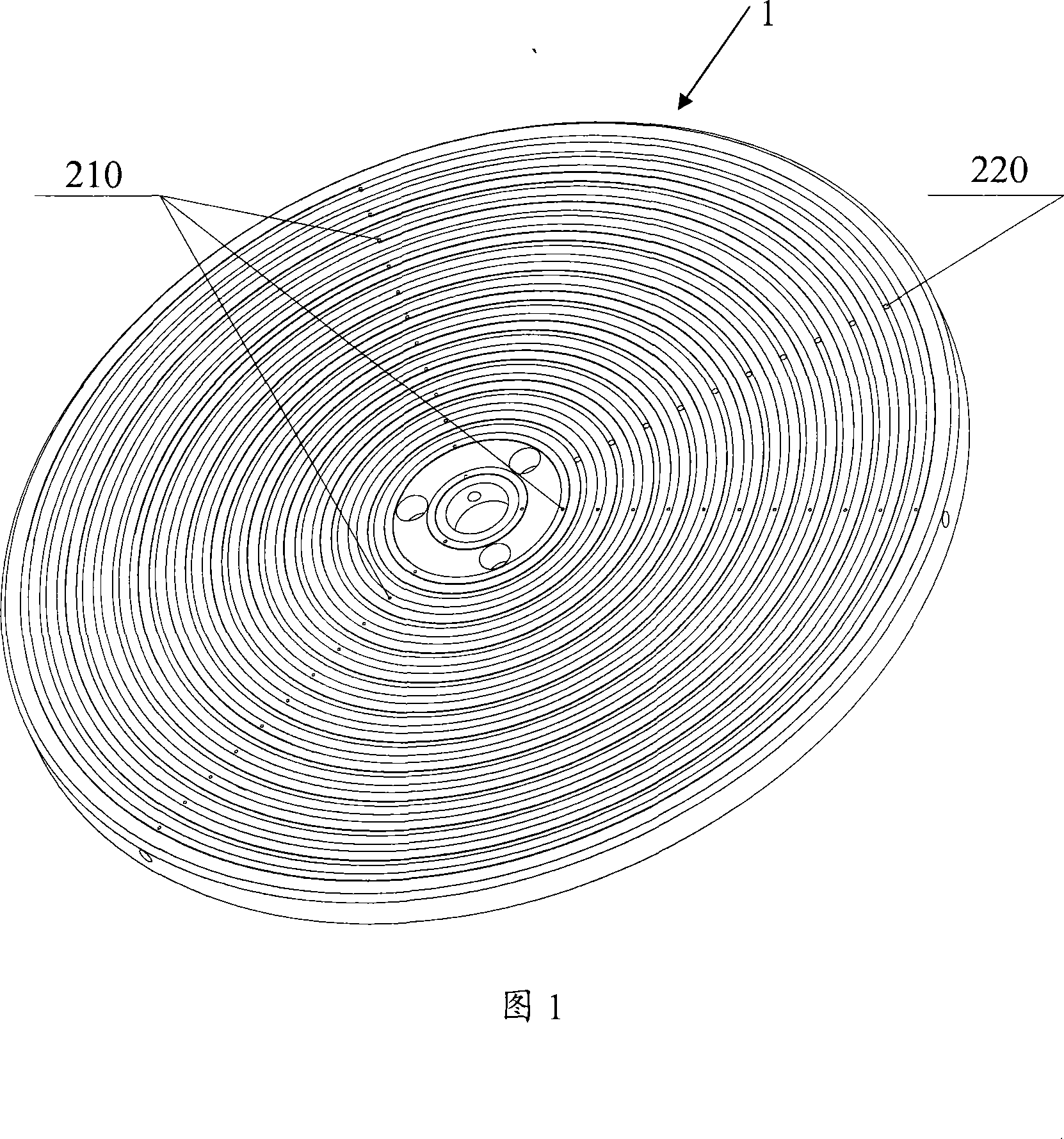
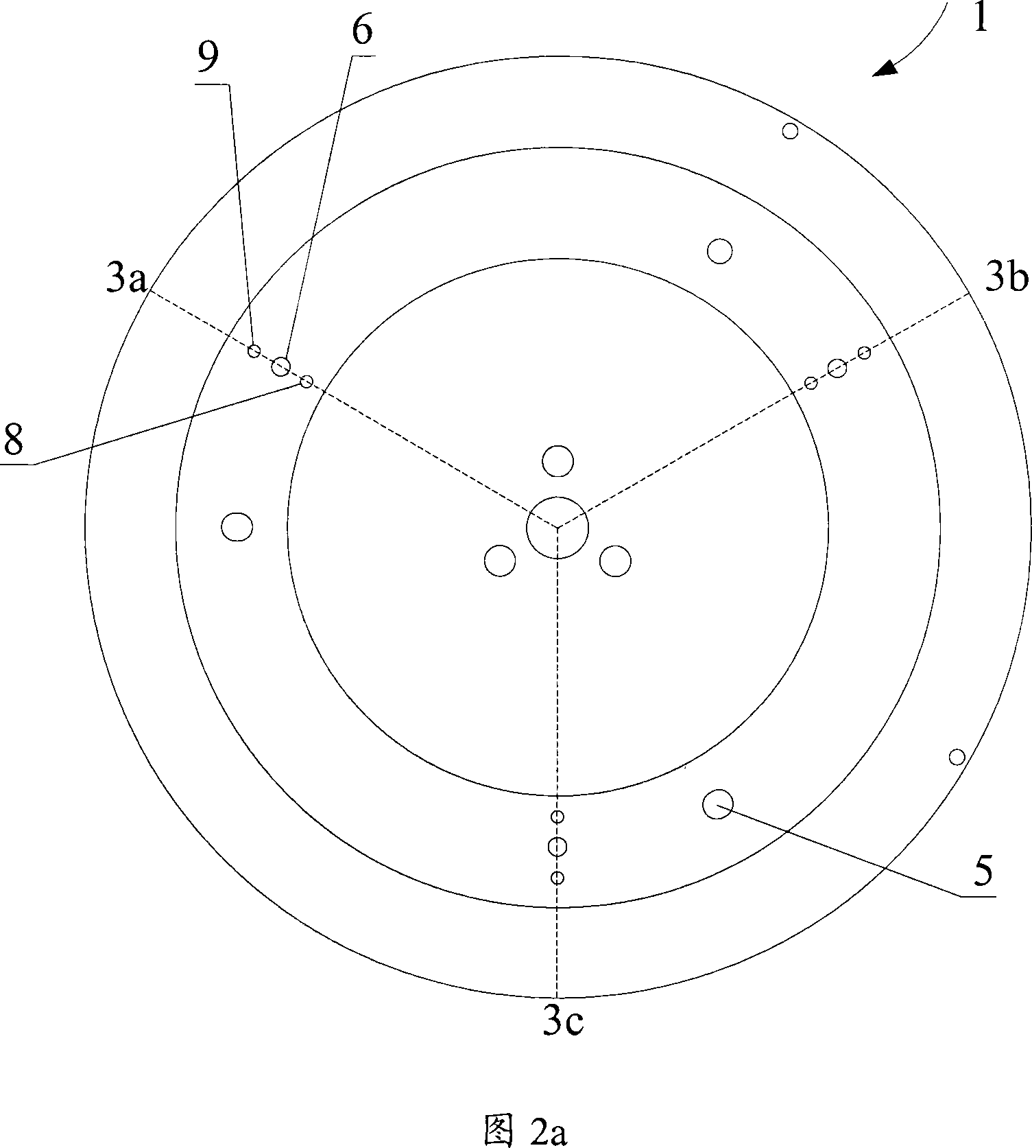
[0020] FIG. 1 is a perspective view of a silicon wafer fixing component 1 provided by the present invention. Please refer to FIG. 1 and in conjunction with FIGS. 3 to 4 , the surface (defined as the adsorption surface) 10 of the silicon wafer fixing component 1 for absorbing silicon wafers is provided with several concentric annular grooves 2 evenly distributed. The depths of the annular grooves 2 are the same, and the cross-sections are designed to be trapezoidal. In this embodiment, an isosceles trapezoid with a base angle of about 45° is adopted. This concave-convex structure reduces the deformation of the silicon wafer fixing part 1 itself, and facilitates processing. By setting the cross section i...


PUM


Abstract

The invention discloses a silicon wafer fixing component, which comprises a plurality of vacuum absorption holes for absorbing silicon wafers, vacuum through holes for communicating the vacuum absorption holes and a plurality of concentric annular grooves for supporting the silicon wafer. The annular groove comprises a vacuum groove and an atmosphere groove arranged at interval in turn, the vacuum absorption hole is positioned in the vacuum groove. The silicon wafer fixing component is also provided with a technics hole isolating the vacuum through hole, the vacuum through hole is isolated after the technics hole is filled, when the technics hole internal side is communicated with the gas controlling device, the technics hole can be used for absorbing No. eight silicon wafer; when both the internal and external sides of the technical hole are communicated, the technics hole can be used for absorbing No. 12 silicon wafer. The atmosphere groove is also internally provided with an atmosphere through hole, the atmosphere through hole can discharge atmosphere between the silicon wafer and the absorption surface, so as to reduce the deformation of the silicon wafer. In addition, by considering the processing manufacturability, the annular groove can be designed into a trapezoid to reduce the processing deformation. The silicon fixing component adopts silicon carbide precision ceramic as the material, the technics performance of the silicon fixing component is improved and the service life is prolonged.

Description

technical field [0001] The invention relates to a silicon wafer stage on an exposure device in the semiconductor field, in particular to a silicon wafer fixing part on the silicon wafer stage. Background technique [0002] In the silicon wafer exposure process, in order to form precise circuit patterns on the surface of the silicon wafer, it is necessary to precisely control the position of the silicon wafer. During exposure, the silicon wafer is placed on the silicon wafer stage and fixed by the fixing parts on the silicon wafer stage. In the prior art, the structures of the fixing components are varied. U.S. Patent No. 6,822,730 discloses a method for designing and manufacturing a silicon wafer stage. The fixing part involved in this document is a magnet adsorption ring, and the silicon wafer stage fixes the silicon wafer by pressing the magnet adsorption ring. This method is not easy to grasp The size of the pressure is easy to crush the silicon wafer. [0003] U.S. Pa...

Claims


Application Information

Patent Timeline
Patent Type & Authority Applications(China)
IPC IPC(8): G03F7/20H01L21/027
Inventor 董同社李志龙
Owner SHANGHAI MICRO ELECTRONICS EQUIP (GRP) CO LTD
Why Eureka
Try Eureka