Package structure and packaging process

A technology of packaging structure and electronic components, applied in the direction of circuit heating devices, electrical components, circuits, etc., can solve the problems of complex packaging structure, poor heat dissipation efficiency of traditional packaging structure, high cost of packaging method, etc.

Pending Publication Date: 2020-05-19
DELTA ELECTRONICS INTL SINGAPORE
View PDF13 Cites 4 Cited by
  • Summary
  • Abstract
  • Description
  • Claims
  • Application Information

AI Technical Summary

Problems solved by technology

However, when the electronic components embedded in the insulating layer of the embedded package structure generate a large amount of heat energy during operation, the heat energy may only dissipate from a single direction, making the heat dissipation efficiency of the traditional package structure not good
In addition, the traditional packaging structure is not only complicated but also the cost of the packaging method is high

Method used


Image

  • Package structure and packaging process
  • Package structure and packaging process
  • Package structure and packaging process

Examples


Embodiment Construction

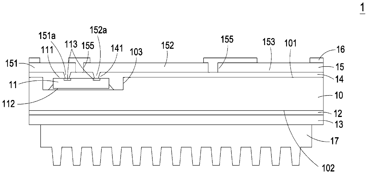
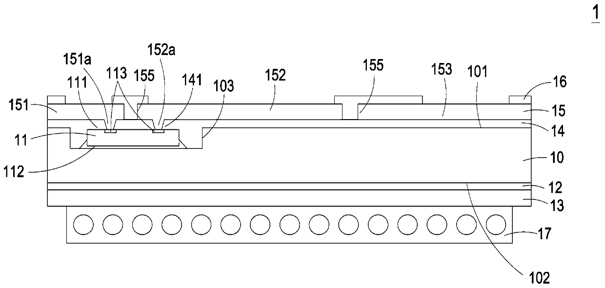
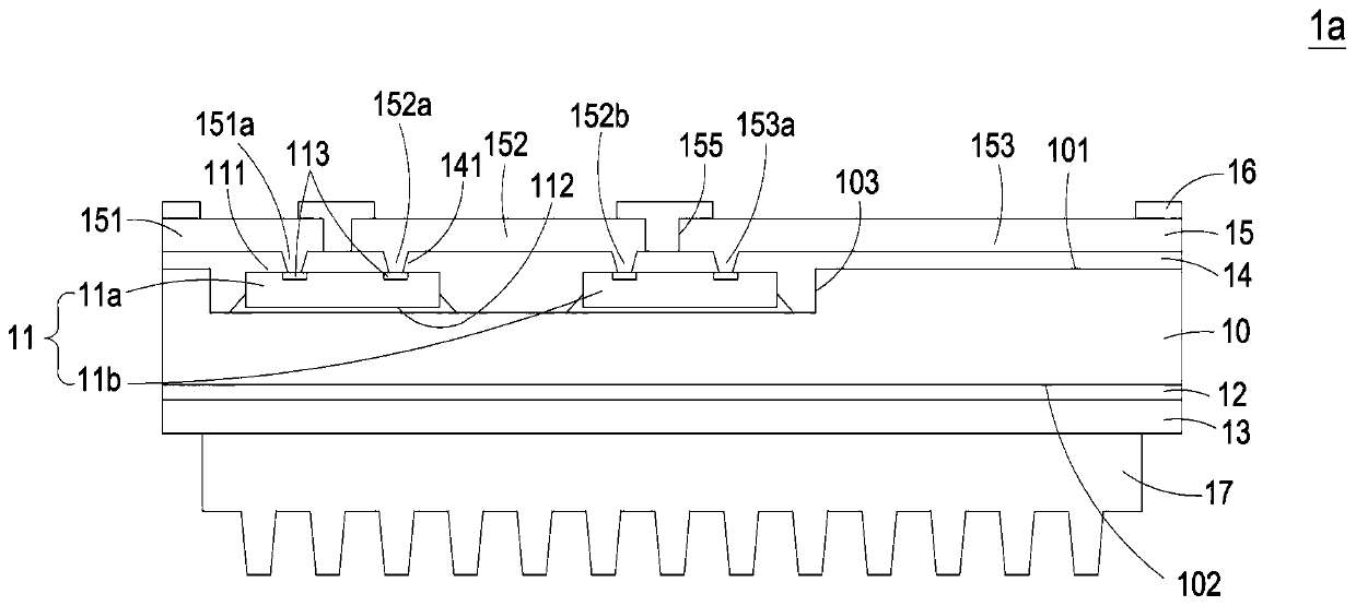
[0056] Some typical embodiments embodying the features and advantages of the present invention will be described in detail in the following description. It should be understood that the present invention can have various changes in different ways, which do not depart from the scope of the present invention, and the descriptions and diagrams therein are essentially for illustrative purposes, rather than being constructed to limit the present invention. invention. For example, if the following disclosure in this specification describes forming a first feature on or above a second feature, it means that it includes an embodiment in which the formed first feature and the second feature are in direct contact It also includes embodiments in which additional features can be formed between the first feature and the second feature, so that the first feature and the second feature may not directly contact. In addition, different embodiments in the description of the present invention ma...


PUM


Abstract

The present invention provides a packaging structure. The package structure includes a carrier, at least one electronic component, a first insulation layer, a heat spreading layer, a second insulationlayer, plural re-distribution blocks, a passivation layer, and a heat dissipation device. The electronic component is disposed in a recess of the carrier and has plural conducting terminals. The first insulation layer is formed on a second surface of the carrier. The heat spreading layer is formed on the first insulation layer. The second insulation layer is formed on a first surface of the carrier. The re-distribution blocks are formed on the second insulation layer. Each re-distribution block includes at least one conductive via disposed in the second insulation layer and in contact with corresponding one of the conductive terminals. The passivation layer is formed on the re-distribution blocks and covers portions of the re-distribution blocks. The heat dissipation device is disposed onthe heat spreading layer.

Description

Technical field [0001] The present invention relates to a packaging structure and a packaging method, in particular to a packaging structure capable of improving heat dissipation efficiency and achieving compactness, and a packaging method used for the packaging structure. Background technique [0002] In recent years, the design of electronic devices has developed towards a trend of small size, lightness and easy portability. Furthermore, with the increasing advancement of electronic industry technology, the internal circuits of electronic devices have gradually developed towards modularization, in other words, multiple electronic components are integrated into a single circuit module. For example, a power module is one of the widely used electronic modules. The power module may include, for example, but not limited to, a DC to DC converter and a DC to AC converter. Or AC to DC converter (AC to DC converter). After multiple electronic components (such as capacitors, resistors,...

Claims


Application Information

Patent Timeline
Patent Type & Authority Applications(China)
IPC IPC(8): H01L25/16H01L23/495H01L23/367H01L21/48
CPCH01L25/165H01L23/3672H01L21/4882H01L23/49568H01L23/13H01L23/492H01L23/36H01L25/105H01L2224/24137H01L2224/24195H01L2224/04105H01L2224/73267H01L2924/15153H01L2224/92244H01L2924/19105H01L2224/32245H01L2225/1035H01L24/24H01L24/19H01L24/32H01L24/73H01L24/92H01L23/5389H01L23/142H01L23/50H01L24/09H05K1/0209H01L2224/02372H01L23/5226H01L23/49861H01L23/367
Inventor 林平平
Owner DELTA ELECTRONICS INTL SINGAPORE
Why Eureka
Try Eureka