A kind of semiconductor chip and semiconductor laser

A technology of semiconductors and lasers, applied in the field of semiconductor chips and semiconductor lasers, can solve problems such as the inability to achieve high beam quality external cavity laser output, and achieve the effects of beam quality output, reduced process difficulty, and efficient overlapping

Active Publication Date: 2021-02-26
TECHNICAL INST OF PHYSICS & CHEMISTRY - CHINESE ACAD OF SCI
View PDF1 Cites 0 Cited by
  • Summary
  • Abstract
  • Description
  • Claims
  • Application Information

AI Technical Summary

Problems solved by technology

However, the applicant found in the process of further research on the semiconductor laser with wide ridges that the structure of the semiconductor chip has a high impact on the electro-optical efficiency of the semiconductor laser. If the existing semiconductor chip is used, it is impossible to achieve an effective high beam. Quality external cavity laser output

Method used


Image

  • A kind of semiconductor chip and semiconductor laser
  • A kind of semiconductor chip and semiconductor laser
  • A kind of semiconductor chip and semiconductor laser

Examples


Embodiment Construction

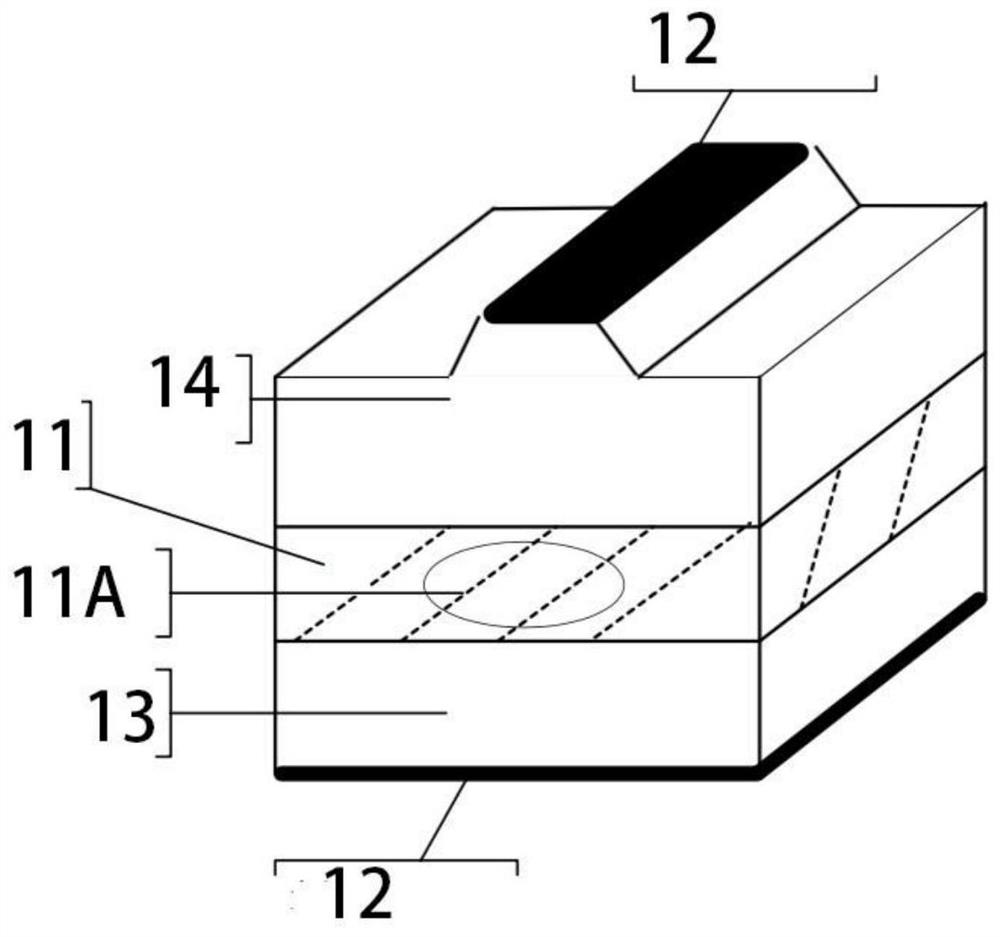
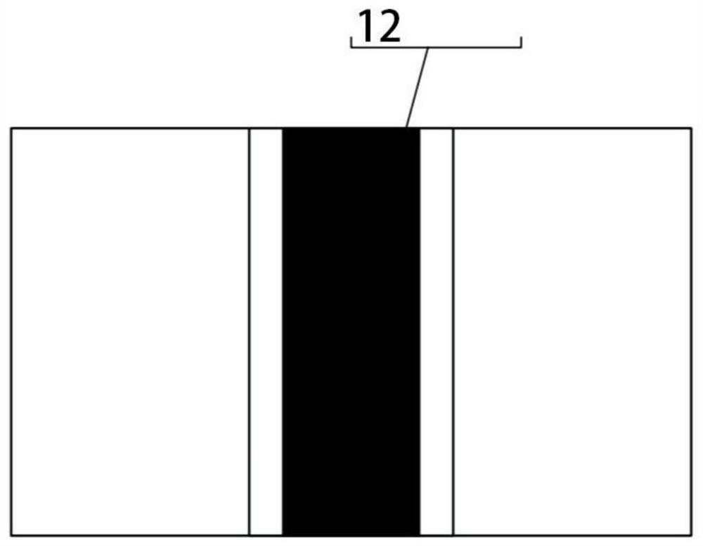
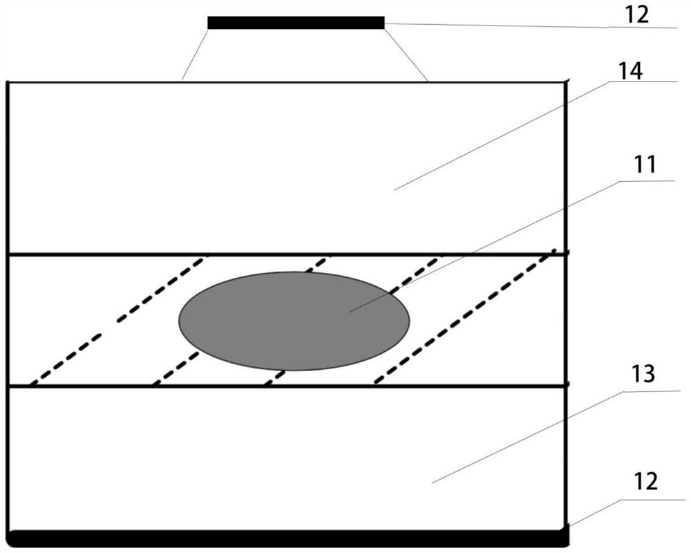
[0036] In order to make the object, technical solution and advantages of the present invention clearer, the present invention will be further described in detail below in combination with specific embodiments and with reference to the accompanying drawings. It should be understood that these descriptions are exemplary only, and are not intended to limit the scope of the present invention. Also, in the following description, descriptions of well-known structures and techniques are omitted to avoid unnecessarily obscuring the concept of the present invention.

[0037] A schematic structural diagram of a semiconductor laser according to an embodiment of the present invention is shown in the accompanying drawings. The figures are not drawn to scale, with certain details exaggerated and possibly omitted for clarity. The shapes of the various regions and layers shown in the figure, as well as their relative sizes and positional relationships are only exemplary, and may deviate due ...


PUM

PropertyMeasurementUnit
angleaaaaaaaaaa
widthaaaaaaaaaa
transmittivityaaaaaaaaaa

Abstract

The invention discloses a semiconductor chip and a semiconductor laser. The semiconductor chip is used to be arranged in the semiconductor laser, comprising: at least one gain region; the upper surface and the lower surface of each gain region are coated with electrodes; at least One of said electrodes is shaped to match the optical path of laser light resonating in said gain region. On the one hand, in the semiconductor chip provided by the embodiment of the present invention, the shape of the electrode is set to match the optical path of the laser resonating in the gain region, which can realize efficient overlapping of the gain region and the external cavity laser mode; on the other hand, the structure can realize the external cavity The gain length of the cavity is much longer than the gain length of the cavity and the maximum width of the amplification of spontaneous emission (ASE). At the same time, it can also cooperate with the coating technology to increase the laser threshold of the cavity, thereby suppressing the laser and ASE of the cavity, and realizing an external cavity semiconductor with high efficiency and high beam quality. Laser output. At the same time, there is no need to etch the ridges, which can reduce the cost and avoid the resulting modulation effect of the external cavity laser on the chip.

Description

technical field [0001] The invention relates to the technical field of laser devices, in particular to a semiconductor chip and a semiconductor laser. Background technique [0002] Semiconductor lasers use semiconductor materials as the gain medium, use electrons to transition between energy levels to emit light, and directly use parallel mirrors formed on the cleavage surface of semiconductor crystals to form a resonant cavity, and form optical oscillation feedback under electrical injection to generate light radiation amplification. Achieve laser output. Semiconductor lasers have the highest electro-optical conversion efficiency among current lasers, and the electro-optical conversion efficiency can reach 70%. And the semiconductor laser is also the laser with the widest wavelength range, the strongest adaptability and reliability, and the lowest mass production cost. However, due to the small size of the resonant cavity of the semiconductor laser (usually millimeter-sca...

Claims


Application Information

Patent Timeline
Patent Type & Authority Patents(China)
IPC IPC(8): H01S5/042H01S5/14
CPCH01S5/0425H01S5/14
Inventor 王小军宗楠彭钦军许祖彦杨晶薄勇
Owner TECHNICAL INST OF PHYSICS & CHEMISTRY - CHINESE ACAD OF SCI
Why Eureka
Try Eureka