Conductive substrate, preparation method thereof and electrochromic device
A technology of electrochromic devices and conductive substrates, applied in instruments, nonlinear optics, optics, etc., can solve the problems of large electron transmission resistance, different electron speeds, slow discoloration speed, etc., and achieve fast conduction speed and uniform voltage distribution. , the effect of improving the stability of service life and performance
- Summary
- Abstract
- Description
- Claims
- Application Information
AI Technical Summary
Problems solved by technology
Method used
Image

Examples
Embodiment 1
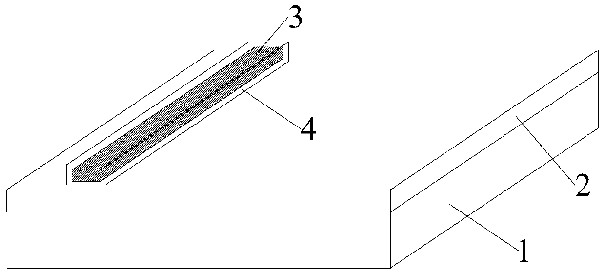
[0062] This embodiment provides a conductive substrate, the structure of the conductive substrate is as follows figure 1 As shown, it includes a transparent conductive base material, a conductive part 3 and an insulating part 4 covering the conductive part 3; the transparent conductive base material includes a transparent conductive layer 2 and a transparent base layer 1 stacked in sequence; the conductive The portion 3 is provided on the surface of the transparent conductive layer 2 .
[0063] The transparent base layer 1 is glass; the transparent conductive layer 2 is an indium tin oxide layer with a thickness of 500 nm; the light transmittance of the transparent conductive substrate is ≥ 70%.
[0064] The material used for the conductive part 3 is conductive silver paste, and the conductive part 3 is arranged along one side edge of the surface of the transparent conductive layer 2, and is in the shape of a strip of equal width, with a width of 10 mm and a thickness of 30 μm...
Embodiment 2
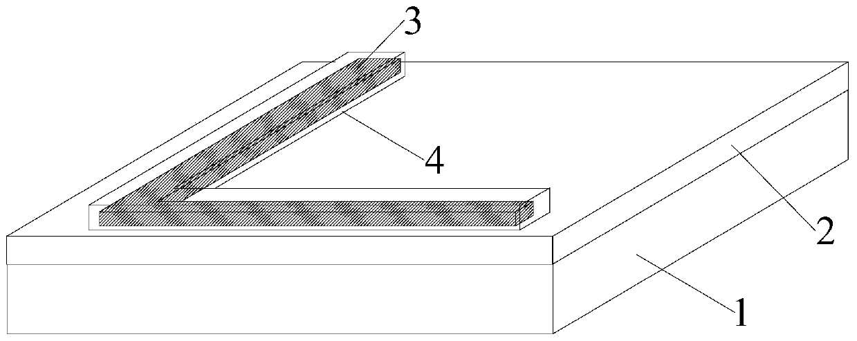
[0070] This embodiment provides a conductive substrate, the structure of the conductive substrate is as follows figure 2 As shown, it includes a transparent conductive base material, a conductive part 3 and an insulating part 4 covering the conductive part 3; the transparent conductive base material includes a transparent conductive layer 2 and a transparent base layer 1 stacked in sequence; the conductive The portion 3 is provided on the surface of the transparent conductive layer 2 .
[0071] The transparent base layer 1 is a flexible base layer of cycloolefin copolymer with a thickness of 250 μm; the transparent conductive layer 2 is an aluminum oxide zinc layer with a thickness of 1 nm; the light transmittance of the transparent conductive base material is ≥ 70%.
[0072] The material used for the conductive part 3 is conductive carbon paste, and the conductive part 3 is arranged along the two side edges of the surface of the transparent conductive substrate in an L shape...
Embodiment 3
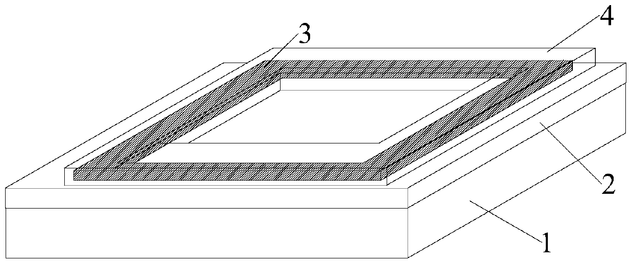
[0078] This embodiment provides a conductive substrate, the structure of the conductive substrate is as follows image 3As shown, it includes a transparent conductive base material, a conductive part 3 and an insulating part 4 covering the conductive part 3; the transparent conductive base material includes a transparent conductive layer 2 and a transparent base layer 1 stacked in sequence; the conductive The portion 3 is provided on the surface of the transparent conductive layer 2 .
[0079] The transparent base layer 1 is a PET layer with a thickness of 120 μm; the transparent conductive layer 2 is a nano-silver layer with a thickness of 1 μm; the light transmittance of the transparent conductive substrate is ≥ 70%.
[0080] The material used for the conductive part 3 is conductive copper paste, and the conductive part 3 is arranged along the four side edges of the surface of the transparent conductive substrate in the shape of a "mouth"; the width of each side of the "mout...
PUM
| Property | Measurement | Unit |
|---|---|---|
| Thickness | aaaaa | aaaaa |
| Thickness | aaaaa | aaaaa |
| Width | aaaaa | aaaaa |
Abstract
Description
Claims
Application Information
 - R&D
- Intellectual Property
- Life Sciences
- Materials
- Tech Scout
- Unparalleled Data Quality
- Higher Quality Content
- 60% Fewer Hallucinations
Browse by: Latest US Patents, China's latest patents, Technical Efficacy Thesaurus, Application Domain, Technology Topic, Popular Technical Reports.
© 2025 PatSnap. All rights reserved.Legal|Privacy policy|Modern Slavery Act Transparency Statement|Sitemap|About US| Contact US: help@patsnap.com