Semiconductor integrated circuit device

An integrated circuit and semiconductor technology, applied in the field of semiconductor integrated circuit devices, can solve the problems that the integrated circuit chip cannot be reduced indefinitely, the main body of the integrated circuit board can accommodate limited space, and achieve the effect of preventing damage

Pending Publication Date: 2020-05-29
四川豪威尔信息科技有限公司
View PDF9 Cites 0 Cited by
  • Summary
  • Abstract
  • Description
  • Claims
  • Application Information

AI Technical Summary

Problems solved by technology

[0004] Aiming at the deficiencies of the prior art, the present invention provides a semiconductor integrated circuit device, which solves the problem that the integrated circuit chip ca...

Method used


Image

  • Semiconductor integrated circuit device
  • Semiconductor integrated circuit device
  • Semiconductor integrated circuit device

Examples


Embodiment Construction

[0025] The following will clearly and completely describe the technical solutions in the embodiments of the present invention with reference to the accompanying drawings in the embodiments of the present invention. Obviously, the described embodiments are only some, not all, embodiments of the present invention. Based on the embodiments of the present invention, all other embodiments obtained by persons of ordinary skill in the art without making creative efforts belong to the protection scope of the present invention.

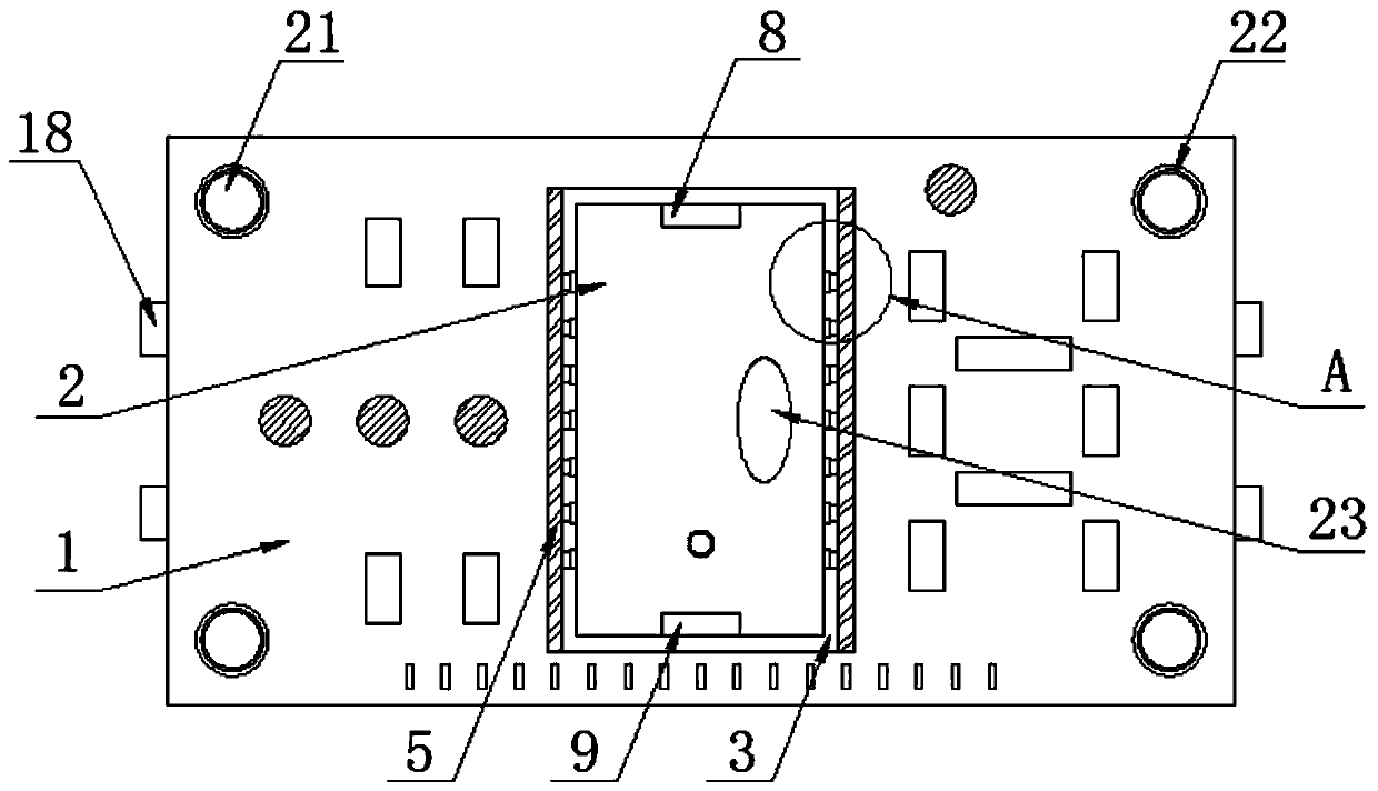
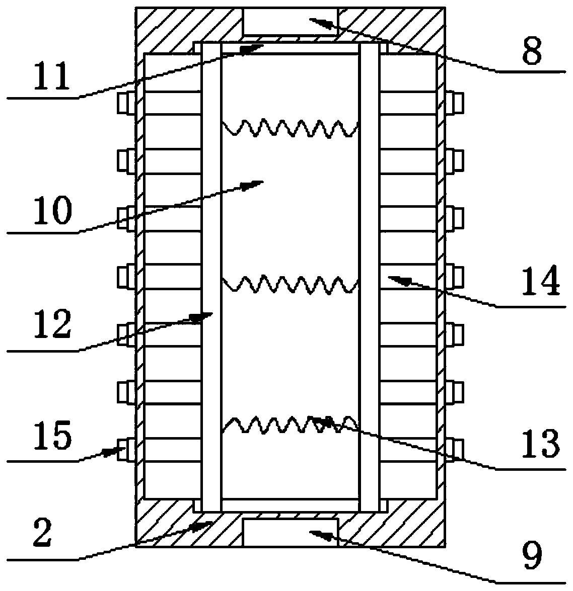
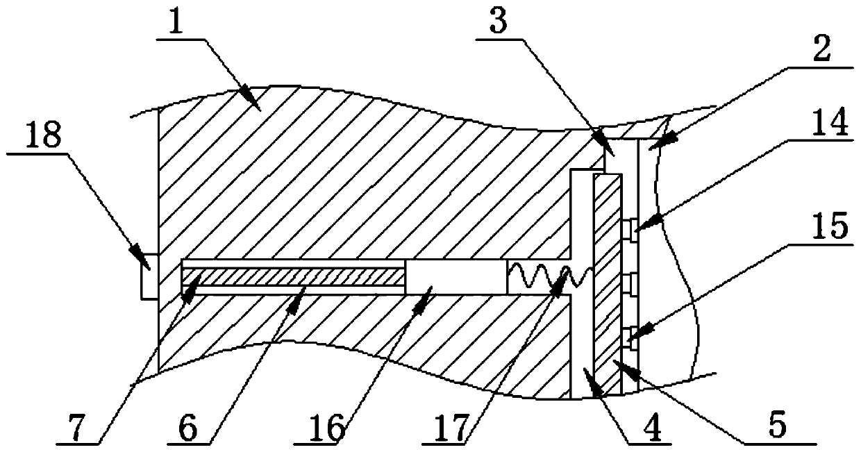
[0026] see Figure 1-7, the present invention provides a technical solution: a semiconductor integrated circuit device, comprising a circuit board main body 1, an integrated circuit chip 2 and a LOGO mark 23, the front of the circuit board main body 1 is provided with a fixing hole 21, and the front of the fixing hole 21 is fixedly connected to There is a protective pad 22, and the protective pad 22 is set to prevent the fixture from damaging the circuit board...


PUM


Abstract

The invention discloses a semiconductor integrated circuit device. The device comprises a circuit board main body, an integrated circuit chip and a LOGO sign; a mounting groove is formed in the frontsurface of the circuit board main body; moving grooves are formed in two sides of the inner cavity of the mounting groove in a communicated manner; baffles are slidably connected to the interiors of the two moving grooves. The invention belongs to the semiconductor technical field. According to the semiconductor integrated circuit device, the mounting groove is adopted, so that an integrated circuit chip is mounted in the mounting groove; compared with a mode in which the integrated circuit chip is fixed on the surface of the circuit board main body, the above arrangement of the integrated circuit chip can assist in effectively decreasing the overlapping thickness of the integrated circuit chip and the circuit board main body, so that the circuit board main body can be installed in a small-sized device easily; pins are embedded into clamping holes, the situation that the pins are buckled on the surface of the circuit board main body and occupy the space of the surface of the circuit board main body is avoided; sliding grooves, sliding plates and first springs are adopted, so that the length of metal connecting rods can be adjusted, and therefore, the integrated circuit chip can beconveniently installed on the circuit board main body.

Description

technical field [0001] The invention relates to the technical field of semiconductors, in particular to a semiconductor integrated circuit device. Background technique [0002] A semiconductor device is an electronic device whose conductivity is between a good conductor and an insulator. It uses the special electrical properties of semiconductor materials to complete specific functions. It can be used to generate, control, receive, transform, amplify signals and perform energy conversion. The semiconductor material of semiconductor devices is silicon, germanium or gallium arsenide, which can be used as rectifiers, oscillators, light emitters, amplifiers, photometers and other equipment. To distinguish them from integrated circuits, they are sometimes called discrete devices. The basic structure of most two-terminal devices (ie, crystal diodes) is a PN junction. Semiconductor devices usually use different semiconductor materials, different processes and geometric structures...

Claims


Application Information

Patent Timeline
IPC IPC(8): H01L23/367H05K1/02H05K1/18
CPCH01L23/367H05K1/02H05K1/0271H05K1/183
Inventor 向彦瑾
Owner 四川豪威尔信息科技有限公司
Why Eureka
Try Eureka