Shallow trench isolation structure and manufacturing method thereof
A technology of isolation structure and manufacturing method, which is applied in semiconductor/solid-state device manufacturing, electrical components, circuits, etc., can solve the problems of forming voids and affecting the isolation performance of shallow trench isolation structures, and achieve the effect of improving performance and filling quality
- Summary
- Abstract
- Description
- Claims
- Application Information
AI Technical Summary
Problems solved by technology
Method used
Image

Examples
Embodiment 1
[0046] Such as Figure 1 to Figure 12 As shown, this embodiment provides a method for manufacturing a shallow trench isolation structure, and the method includes the following steps:
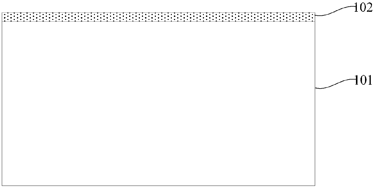
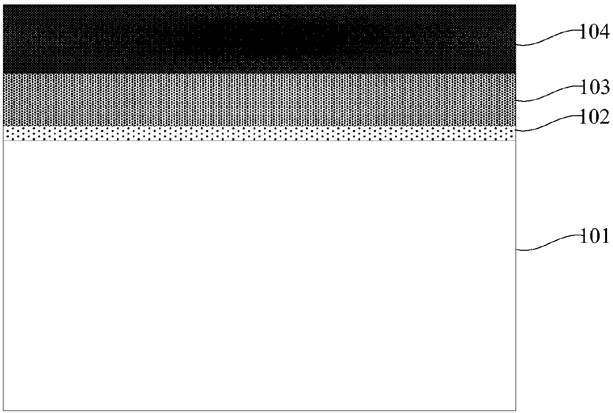
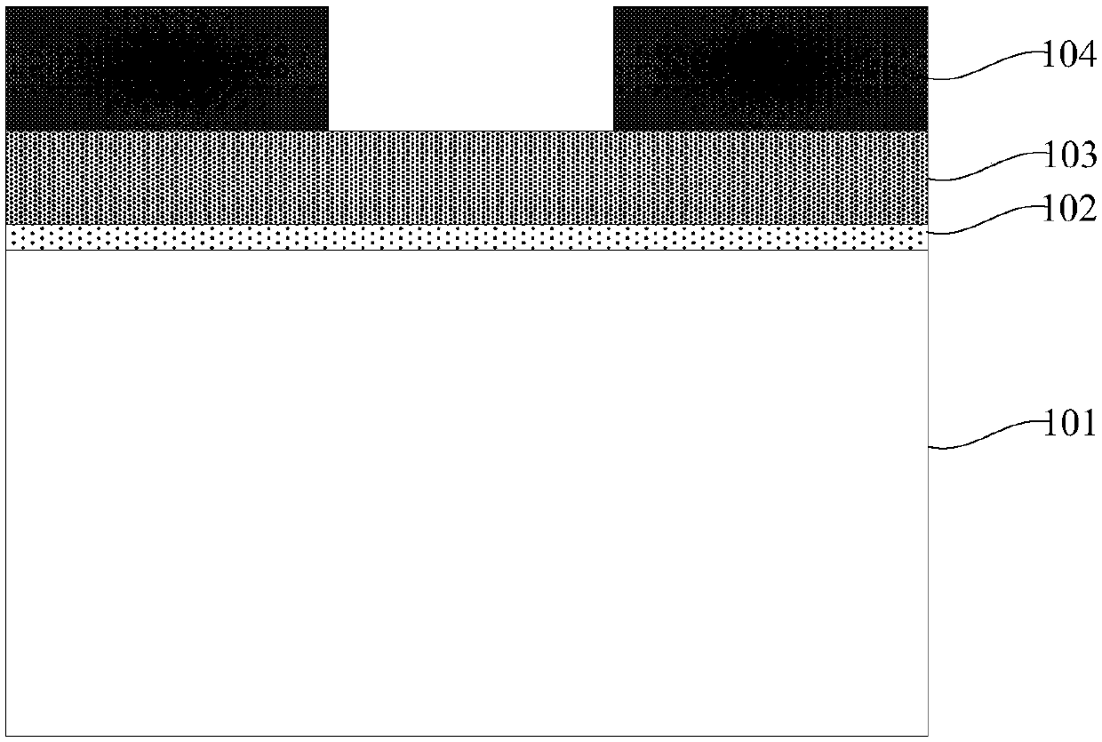
[0047] Such as Figure 1 to Figure 5 As shown, step 1) is first performed, providing a substrate 101, the oxide protection layer 102 is formed on the surface of the substrate 101, and the oxide protection layer 102 and the substrate 101 are patterned and etched, so that the A first trench 105 is formed in the substrate 101 .
[0048] The substrate 101 can be a silicon substrate, a silicon germanium substrate, a silicon carbide substrate, a germanium substrate, etc., and can be doped or undoped. For example, the substrate 101 can be P-type doped Silicon substrate or N-type doped silicon substrate, etc.
[0049] Such as figure 1 As shown, in this example, an oxide protection layer 102 is formed on the surface of the substrate 101, and the oxide protection layer 102 can protect the surface of t...
Embodiment 2
[0066] Such as Figure 12 As shown, this embodiment provides a shallow trench isolation structure, and the shallow trench isolation structure includes a substrate 101 , a first isolation layer 107 and a second isolation layer.
[0067] Such as Figure 12 As shown, the substrate 101 can be a silicon substrate, a silicon germanium substrate, a silicon carbide substrate, a germanium substrate, etc., and can be doped or undoped. For example, the substrate 101 can be P Type doped silicon substrate 101 or N type doped silicon substrate, etc.
[0068] There is a first trench 105 in the substrate 101, and the shallow trench isolation structure further includes an oxide liner layer 106 formed on the bottom and sidewall of the first trench 105, and the oxide liner The pad layer 106 is located between the substrate 101 and the first isolation layer 107, and at the same time, the oxide pad layer 106 is formed on the top corner of the first trench 105, so that the first trench The apex ...
PUM
| Property | Measurement | Unit |
|---|---|---|
| thickness | aaaaa | aaaaa |
Abstract
Description
Claims
Application Information