Manufacturing method of 3D storage device and chemical vapor deposition method of adhesive film

A technology of chemical vapor deposition and manufacturing method, which is applied in semiconductor/solid-state device manufacturing, gaseous chemical plating, electrical components, etc. It can solve the problems that the precursor gas is difficult to reach the bottom of the deposition channel, device failure, etc., and achieve improved electrical performance , Improve adhesion, increase the effect of step coverage

Active Publication Date: 2022-05-31
YANGTZE MEMORY TECH CO LTD
View PDF5 Cites 0 Cited by
  • Summary
  • Abstract
  • Description
  • Claims
  • Application Information

AI Technical Summary

Problems solved by technology

In the process of forming the adhesive film, it is difficult for the precursor gas used to form the adhesive film to reach the bottom of the deposition channel, so that the adhesive film at the bottom of the deposition channel and the lower part of the sidewall is thinner, or even not covered by the adhesive film, thus As a result, the metal material cannot be normally filled in the deposition channel, resulting in device failure

Method used


Image

  • Manufacturing method of 3D storage device and chemical vapor deposition method of adhesive film
  • Manufacturing method of 3D storage device and chemical vapor deposition method of adhesive film
  • Manufacturing method of 3D storage device and chemical vapor deposition method of adhesive film

Examples


Embodiment Construction

[0027] The present invention will be described in more detail below with reference to the accompanying drawings. In the various figures, the same elements are provided with similar labels.

[0029] If in order to describe the situation directly on another layer, another area, the text will use "directly on...

[0030] In this application, the term "semiconductor structure" refers to the entire semiconductor structure formed in the various steps of manufacturing a memory device

[0031] The present invention may be embodied in various forms, some examples of which will be described below.

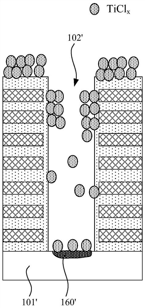
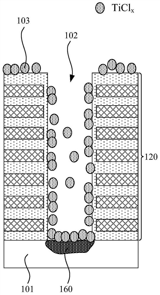
[0032] FIG. 1 shows a schematic diagram of a prior art adhesion film deposition method.

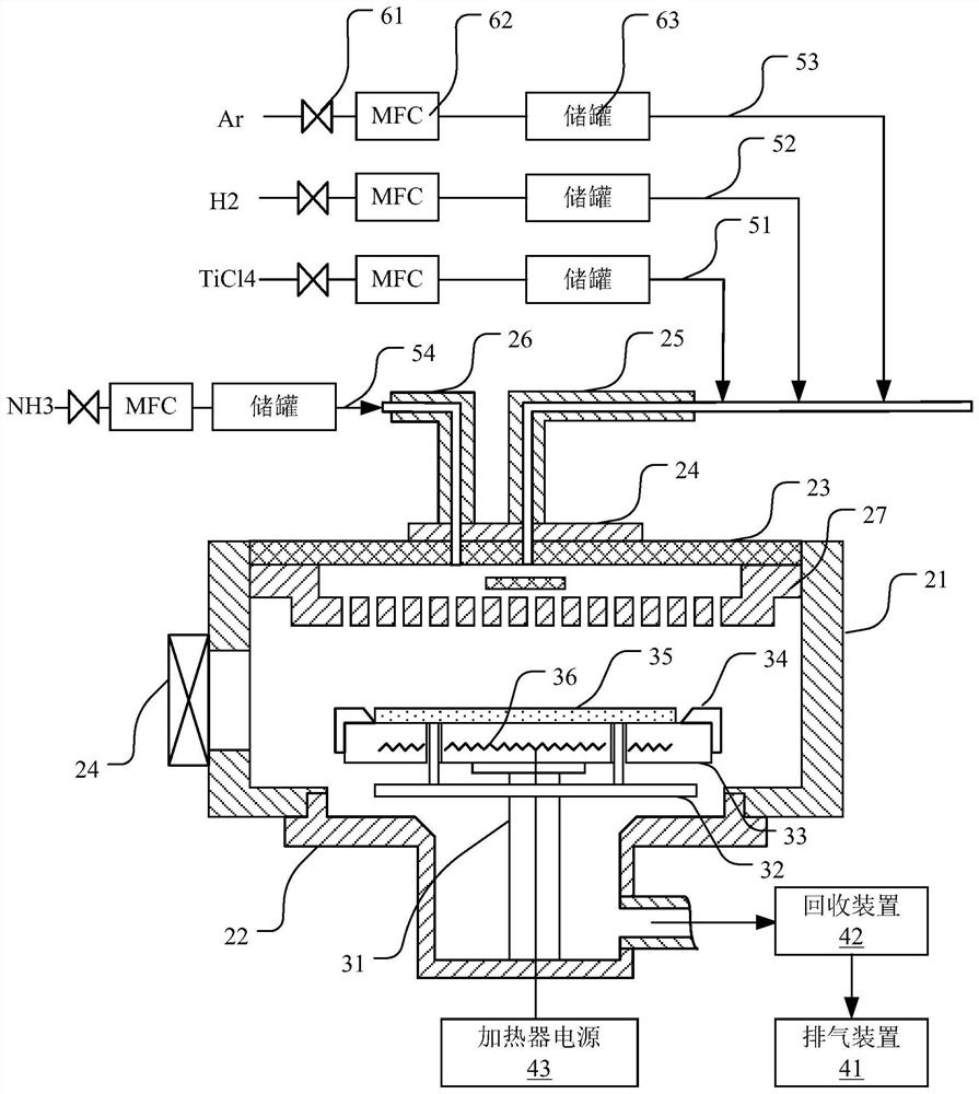
[0033] An adhesive film is formed on a predetermined surface of the semiconductor structure using a chemical vapor deposition process. The deposition method includes

[0036] In a 3D memory device, a TiN film needs to be used as an adhesive film for a metal conductive structure. This is due to deposition ...


PUM


Abstract

The application discloses a manufacturing method of a 3D storage device and a chemical vapor deposition method of an adhesive film. The chemical vapor deposition method includes: placing a semiconductor structure with a deposition channel in a reaction chamber, at least the sidewall of the deposition channel is covered by an oxide layer; 4 The first reaction gas, containing H 2 The second reaction gas and the inert gas, the volume / mass of the first and second reaction gases are preset to a selected ratio; the tail gas is discharged out of the reaction chamber at a preset rate, the first reaction gas, the second reaction gas and the inert gas The reaction produces TiCl x , the second reactant gas with TiCl x The reaction produces a Ti film covering the inner surface of the deposition channel as at least part of the adherent film, and the tail gas includes unreacted TiCl 4 with TiCl x , when the volume / mass ratio of the first reactant gas to the second reactant gas is preset at a selected ratio, the inert gas slows down the TiCl 4 with TiCl x The discharge rate of TiCl reaches the bottom and sidewall of the deposition channel x evenly distributed.

Description

Manufacturing method of 3D memory device and chemical vapor deposition method of adhesive film technical field [0001] The present invention relates to the technical field of semiconductor manufacturing, and more particularly, to a manufacturing method and adhesion of a 3D memory device Methods of chemical vapor deposition of films. Background technique [0002] The increase in the storage density of memory devices is closely related to the advancement of semiconductor manufacturing processes. With semiconductor manufacturing The feature size of the process is getting smaller and smaller, and the storage density of the memory device is getting higher and higher. In order to further increase the storage density, the Three-dimensionally structured memory devices (ie, 3D memory devices) are developed. The 3D memory device consists of multiple stacking along the vertical direction For memory cells, the integration level can be doubled on a wafer per unit area, and the co...

Claims


Application Information

Patent Timeline
Patent Type & Authority Patents(China)
IPC IPC(8): H01L21/205
CPCC23C16/34C23C16/14C23C16/42C23C16/455C23C16/45563C23C16/042C23C16/54H01L21/76843
Inventor 毛格胡凯刘子良
Owner YANGTZE MEMORY TECH CO LTD
Why Eureka
Try Eureka