Parasitic patch array antenna substrate integrated waveguide feed

A waveguide feeding and parasitic patch technology, applied in the direction of electrical short antennas, antennas, resonant antennas, etc., can solve the problems of multi-surface wave loss of radiating patches, narrow antenna bandwidth, and high quality factor, to expand bandwidth and increase bandwidth. , Improve the effect of antenna gain

Active Publication Date: 2020-06-05
NANJING UNIV OF AERONAUTICS & ASTRONAUTICS
View PDF10 Cites 2 Cited by
  • Summary
  • Abstract
  • Description
  • Claims
  • Application Information

AI Technical Summary

Problems solved by technology

However, due to its high quality factor, the bandwidth of the antenna is still narrow
And because the radiation patch still has more surface wave loss at high frequencies, its gain is not high

Method used


Image

  • Parasitic patch array antenna substrate integrated waveguide feed
  • Parasitic patch array antenna substrate integrated waveguide feed
  • Parasitic patch array antenna substrate integrated waveguide feed

Examples


Embodiment Construction

[0029] The present invention will be further described below in conjunction with the accompanying drawings.

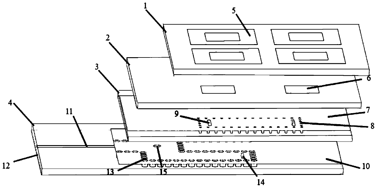
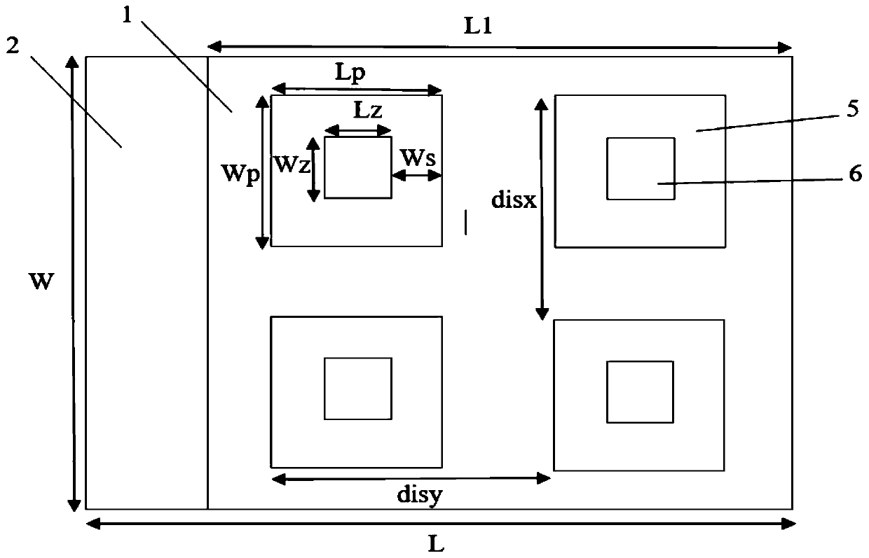
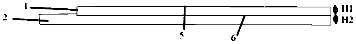
[0030] The substrate-integrated waveguide-fed parasitic patch array antenna of the present invention includes a first dielectric plate 1, a second dielectric plate 2, a third dielectric plate 3 and a fourth dielectric plate 4, wherein the first dielectric plate 1 is located on the second dielectric plate 2, the second dielectric plate 2 is located above the third dielectric plate 3, and the third dielectric plate 3 is located above the fourth dielectric plate 4. Four annular patches 5 arranged in two rows and two columns are arranged above the first dielectric plate 1, and four main radiation patches 6 arranged in two rows and two columns are arranged above the second dielectric plate 2. The pieces 6 are located directly below the annular patches 5 in one-to-one correspondence. The upper surface of the third dielectric plate 3 is the first metal layer 7, and the first...


PUM

PropertyMeasurementUnit
widthaaaaaaaaaa
thicknessaaaaaaaaaa
thicknessaaaaaaaaaa

Abstract

The invention discloses a parasitic patch array antenna with substrate integrated waveguide feed. The parasitic patch array comprises a first dielectric plate, a second dielectric plate, a third dielectric plate and a fourth dielectric plate. The parasitic patch array is characterized in that the first dielectric plate is positioned above the second dielectric plate; the second dielectric plate ispositioned above the third dielectric plate; and the third dielectric plate is positioned above the fourth dielectric plate. The first dielectric plate is provided with an annular patch; the second dielectric plate is provided with a main radiation patch; metal through hole structures on the third dielectric plate and the fourth dielectric plate form a one-to-four substrate integrated waveguide feed network, and feed is carried out on the main radiation patch through a gap in the third dielectric plate. The annular patch plays a guiding role, and the substrate integrated waveguide feed network plays a role in reducing feed loss. The array antenna overcomes the defects of large feed loss and low gain of a microstrip patch array antenna, has the advantages of low profile, small size and easiness in planar circuit integration, and can be used for low-profile terahertz or millimeter wave communication.

Description

Technical field: [0001] The invention relates to a substrate-integrated waveguide feeding parasitic patch array antenna, which belongs to the technical field of communication. Background technique: [0002] With the continuous development of communication and information technology, in order to improve the communication rate of the communication system and alleviate the shortage of spectrum resources, more and more researches are being carried out on the millimeter wave and terahertz frequency bands. The antenna is an important part of the wireless communication system. Working in the high frequency band requires the antenna to have relevant characteristics such as small size, high gain, high integration, and easy integration with planar circuits. [0003] The microstrip patch antenna has a planar circuit structure, is easy to integrate with microwave and millimeter wave circuits, and is easy to process and design, but the gain is not high, the bandwidth is narrow, and the m...

Claims


Application Information

Patent Timeline
Patent Type & Authority Applications(China)
IPC IPC(8): H01Q1/38H01Q1/50H01Q9/04H01Q13/10H01Q21/00
CPCH01Q1/38H01Q1/50H01Q9/0407H01Q9/0464H01Q13/10H01Q21/00Y02D30/70
Inventor 井庆丰别雨轩朱忠博
Owner NANJING UNIV OF AERONAUTICS & ASTRONAUTICS
Why Eureka
Try Eureka