
Processing method to obtain asymmetric waveguide structure through processing on optical fiber

An asymmetrical waveguide and processing method technology, applied to metal processing equipment, control of workpiece feed movement, machine tools suitable for grinding workpiece planes, etc., to achieve good repeatability, low cost, and easy-to-master processing procedures

Inactive Publication Date: 2020-06-09
苏州凯文堡尼光电科技有限公司
View PDF7 Cites 0 Cited by
  • Summary
  • Abstract
  • Description
  • Claims
  • Application Information

AI Technical Summary

Problems solved by technology

On the other hand, silicon-on-chip systems are generally constructed on very small silicon chips, and generally require at least three different materials, and require relatively strong professionalism in terms of operation.

Method used


Image

  • Processing method to obtain asymmetric waveguide structure through processing on optical fiber
  • Processing method to obtain asymmetric waveguide structure through processing on optical fiber

Examples


Embodiment Construction

[0021] The present invention is further declared below in conjunction with embodiment, but should not limit protection scope of the present invention with this.

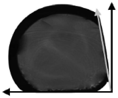
[0022] Table 1 Processing parameters and test results of 3 examples of the present invention.

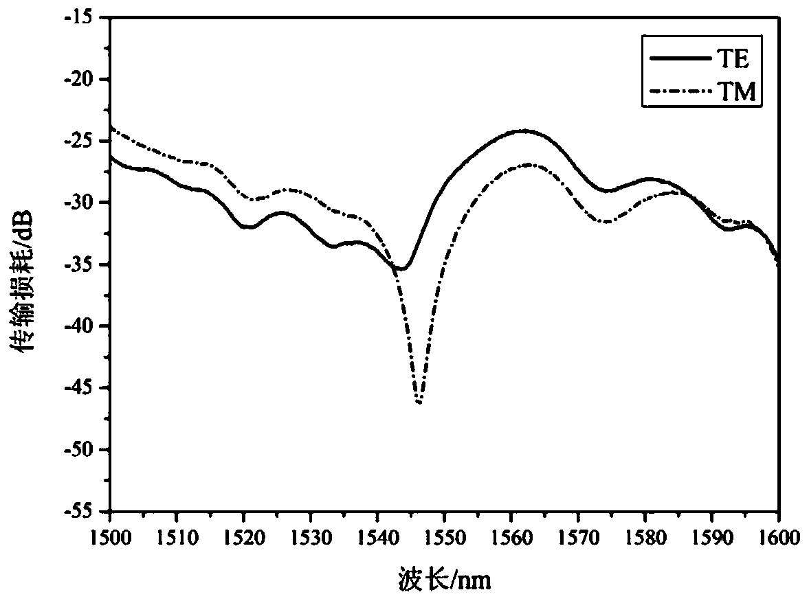
[0023] Sample serial number Example 1 Example 2 Example 3 Polishing Depth (μm) 20 20 20 Polishing Angle(°) 85 65 45 Extinction ratio(dB) 13 7.5 4

[0024] Three embodiments all adopt identical processing mode, and its concrete preparation process is as follows:

[0025] ① Briefly handle the optical fiber to be processed. First peel off the coating layer of the optical fiber to be processed, and then use a dust-free paper dipped in a small amount of alcohol to wipe off the remaining coating debris on the surface of the optical fiber;

[0026] ②Install sandpaper with appropriate roughness on the rollers of the polishing equipment according to actual needs, and ensure that the san...


PUM


Abstract

The invention discloses a processing method to obtain an asymmetric waveguide structure through processing on an optical fiber. The processing method comprises the following steps of 1, briefly processing the optical fiber to be processed; 2, installing abrasive paper on a roller of polishing and grinding equipment; 3, setting a polishing-grinding depth and a polishing-grinding length of the polishing and grinding equipment, and setting a proper rotating speed of the roller; fixing the optical fiber on an optical fiber clamp; 4, monitoring the polishing-grinding depth in real time through a CCD, and carrying out two-face polishing and grinding; and 5, flatly fixing a sample on a glass slide. According to the processing method, the fiber core diameter of the multimode optical fiber used is105 mu m, and the cladding diameter is 125 mu m; an asymmetric structure construction method is adopted, used materials are low in manufacturing cost, machining procedures are easy to master, repeatability is good, and accordingly quantitative production can be realized; and besides, an original circular symmetrical structure of the optical fiber is destroyed in the method, so that the asymmetricwaveguide structure has certain polarization dependence so as to own potential values for being used as a polarization control device.

Description

technical field [0001] The invention relates to a processing method for obtaining an asymmetric waveguide structure on an optical fiber. Background technique [0002] At present, there are many ways to control the polarization state. If it is classified from the direction of whether special materials are used, there are two types. One is to cover the waveguide with a material that is sensitive to the polarization state. The existing materials used mainly include graphene, metal, and liquid crystal. [0003] In 2015, Professor Wu Qiang and his team proposed a micro-fiber structure placed on a silver substrate. Through the simulation results, the researchers found that when the plasmonic mode in the microfiber is excited, the TM mode will exhibit greater loss than the TE mode. The experimental results show that the extinction ratio between the TE mode and the TM mode can reach 20 dB. Therefore, a polarizer through which only the TE mode passes is successfully realized throug...

Claims


Application Information

Patent Timeline
Patent Type & Authority Applications(China)
IPC IPC(8): B24B7/10B24B49/12
CPCB24B7/10B24B49/12
Inventor 王鹏飞王若凝田可
Owner 苏州凯文堡尼光电科技有限公司
Learn More