Insulated gate bipolar transistor and preparation method thereof

A bipolar transistor, insulated gate technology, applied in semiconductor/solid-state device manufacturing, semiconductor devices, electrical components, etc., can solve problems such as difficulty in manufacturing FS-IGBT chips

Pending Publication Date: 2020-06-09
EDGELESS SEMICON CO LTD OF ZHUHAI +1
View PDF0 Cites 0 Cited by
  • Summary
  • Abstract
  • Description
  • Claims
  • Application Information

AI Technical Summary

Problems solved by technology

[0003] However, in terms of process technology, in order to achieve the characteristic of field stop, the thickness of the substrate layer must be ground to a very thin level, which has caused great difficulty in the manufacture of the entire FS-IGBT chip.

Method used


Image

  • Insulated gate bipolar transistor and preparation method thereof
  • Insulated gate bipolar transistor and preparation method thereof
  • Insulated gate bipolar transistor and preparation method thereof

Examples


Embodiment Construction

[0041] The following will clearly and completely describe the technical solutions in the embodiments of the present invention with reference to the accompanying drawings in the embodiments of the present invention. Obviously, the described embodiments are only some, not all, embodiments of the present invention. Based on the embodiments of the present invention, all other embodiments obtained by persons of ordinary skill in the art without making creative efforts belong to the protection scope of the present invention.

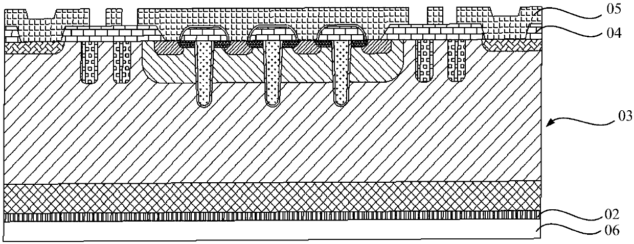
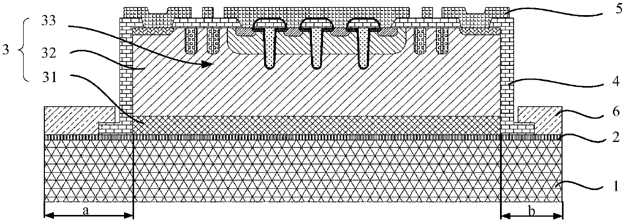
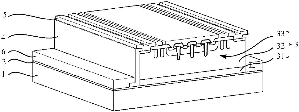
[0042] Please refer to Figure 2 to Figure 3 , a transistor provided by an embodiment of the present invention includes a substrate 1, a collector layer 2 is provided on the substrate 1, a device layer 3 is provided on the side of the collector layer 2 facing away from the substrate 1, and the device layer 3 is arranged on the substrate 1 is smaller than the projected area of ​​the collector layer 2 on the substrate 1, and the projection of the device layer 3 ...


PUM

PropertyMeasurementUnit
thicknessaaaaaaaaaa

Abstract

The invention relates to the technical field of power semiconductor chips, and discloses an insulated gate bipolar transistor and a preparation method thereof. The transistor comprises a substrate; acollector layer and a device layer are arranged on the substrate; the projection of the device layer on the substrate comprises at least two opposite side edges, and a set distance is formed between the side edges and the edge of the projection of the collector layer on the substrate; the outer surface of the device layer is coated with a dielectric layer; an emitter bonding metal layer is formedon the side, away from the device layer, of the dielectric layer; and a collector bonding metal layer is arranged on the side, away from the substrate, of the collector layer and located outside the device layer. In the above transistor, when the transistor is electrified, electrons sequentially pass through the emitter bonding metal layer, the device layer, the collector layer and the collector bonding metal layer, current conduction is realized, so that a current passing path does not pass through the substrate, a thicker substrate can be adopted in the transistor to bear an ultrathin devicelayer, an ultrathin thinning process and related complex steps are not needed, and the manufacturing cost and the manufacturing difficulty are reduced.

Description

technical field [0001] The invention relates to the technical field of power semiconductor chips, in particular to an insulated gate bipolar transistor and a preparation method thereof. Background technique [0002] The insulated gate bipolar transistor FS-IGBT (Field Stop Insulated Gate Bipolar Transistor) with an electric field stop structure is the most advanced IGBT device at present. Because it increases the N-type semiconductor layer structure, the electric field distribution of the device is cut off (Field Stop Insulated Gate Bipolar Transistor) Stop), thereby reducing the thickness of the N-type withstand voltage layer, reducing the conduction voltage drop and power loss of the device. Compared with other PT-IGBT and NPT-IGBT structures, its performance has been greatly improved, and it has gradually become the mainstream design in the IGBT field; the structure of FS-IGBT in the prior art is as follows figure 1 As shown, it includes an emitter bonding metal layer 05...

Claims


Application Information

Patent Timeline
Patent Type & Authority Applications(China)
IPC IPC(8): H01L29/739H01L29/06H01L21/331
CPCH01L29/0611H01L29/66348H01L29/7397H01L29/06H01L29/739
Inventor 史波肖婷曾丹廖勇波敖利波梁博
Owner EDGELESS SEMICON CO LTD OF ZHUHAI
Why Eureka
Try Eureka