Display panel and side surface bonding method thereof

A display panel and bonding technology, applied in the direction of instruments, electrical components, magnetic field/electric field shielding, etc., can solve the problems of weakened electromagnetic shielding effect, poor ICTape coverage, failure, etc., to achieve the effect of ensuring the effect of electromagnetic shielding

Active Publication Date: 2020-06-19
WUHAN CHINA STAR OPTOELECTRONICS SEMICON DISPLAY TECH CO LTD
View PDF21 Cites 2 Cited by
  • Summary
  • Abstract
  • Description
  • Claims
  • Application Information

AI Technical Summary

Problems solved by technology

[0004] In view of this, the present invention provides a display panel and its side bonding method to solve the problem in the prior art that the electromagnetic shielding effect is weakened or even invalidated due to poor coverage of IC Tape due to the height difference of the bonding area on the side of the display panel.

Method used


Image

  • Display panel and side surface bonding method thereof
  • Display panel and side surface bonding method thereof
  • Display panel and side surface bonding method thereof

Examples


Embodiment Construction

[0029] The technical solutions of the embodiments of the present invention will be clearly and completely described below in conjunction with the accompanying drawings. Apparently, the described embodiments are only some, not all, embodiments of the present invention. Based on the embodiments of the present invention, all other embodiments obtained by those skilled in the art without creative efforts fall within the protection scope of the present invention. In the case of no conflict, the following embodiments and technical features thereof can be combined with each other.

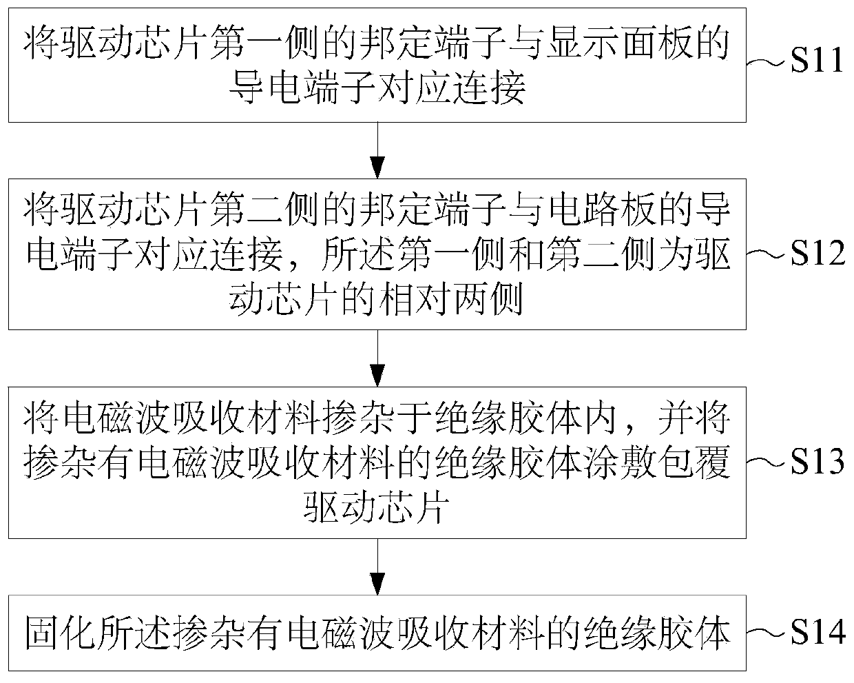
[0030] figure 1 It is a schematic flowchart of a side bonding method of a display panel according to an embodiment of the present invention. see figure 1 As shown, the side bonding method of the display panel includes:

[0031] S11: Correspondingly connect the bonding terminal on the first side of the driving chip to the conductive terminal of the display panel.

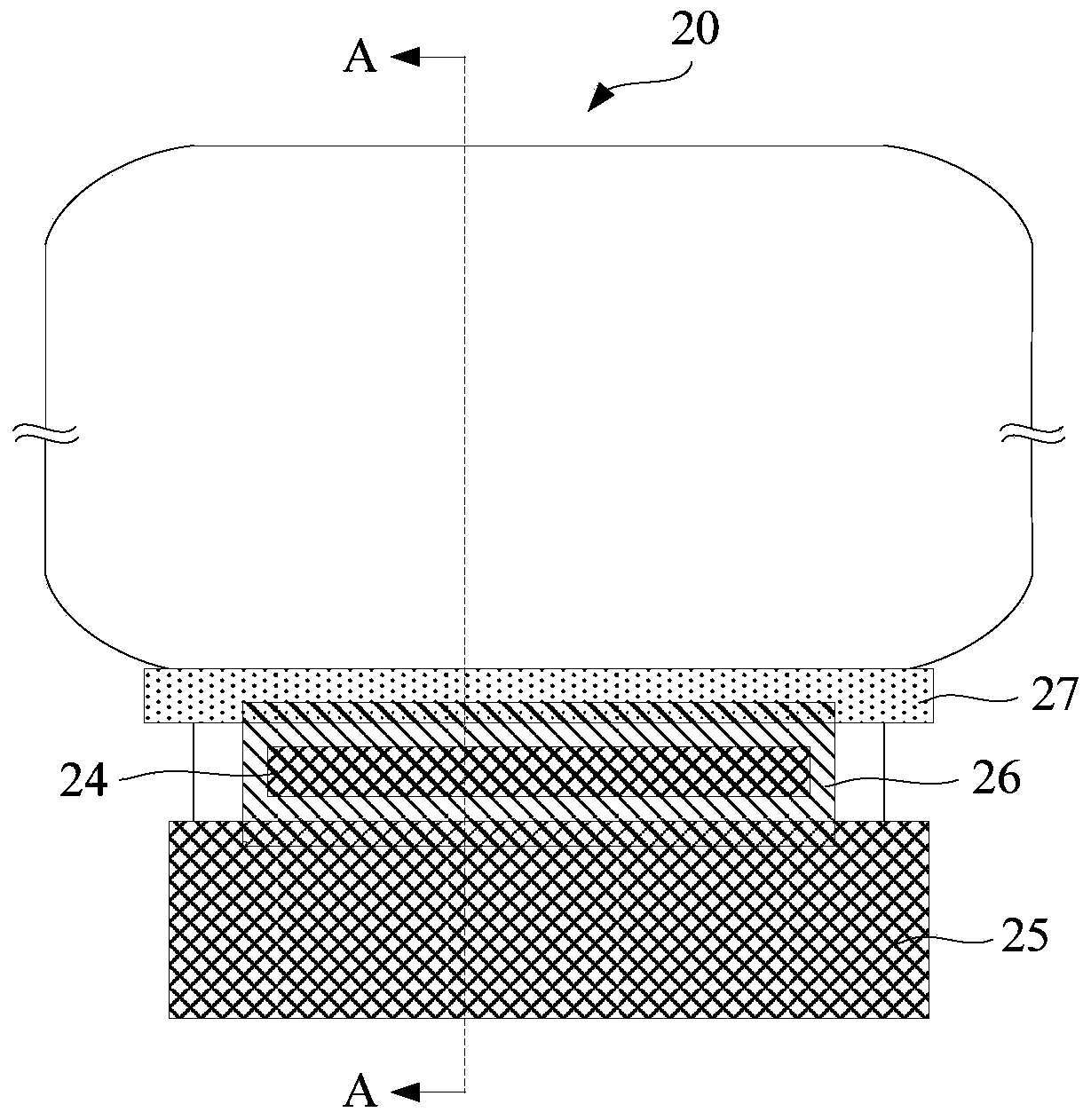
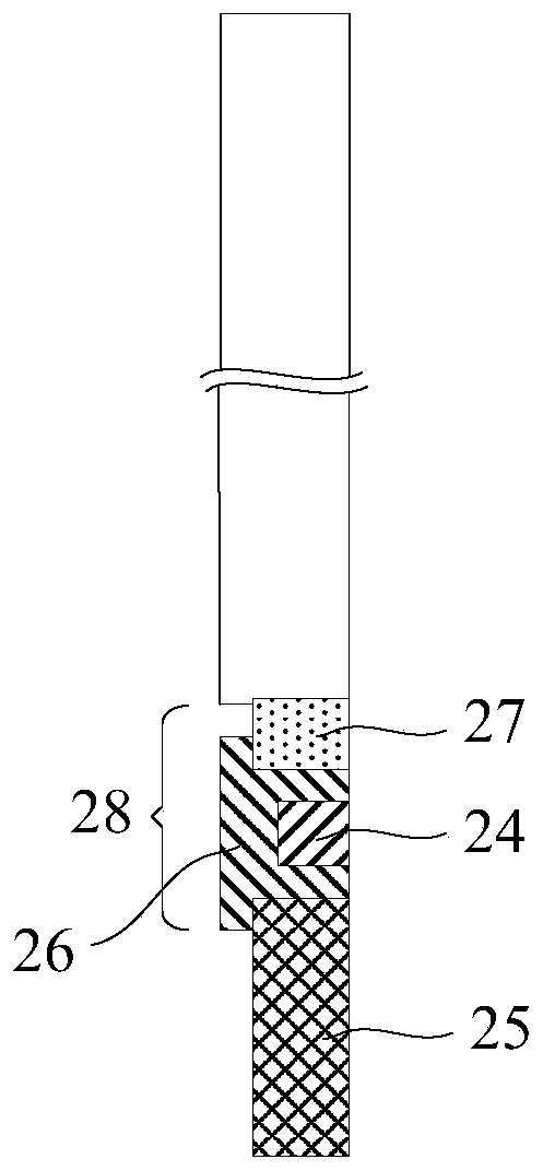
[0032] Please also refer to Figure ...


PUM


Abstract

The invention discloses a display panel and a side surface bonding method thereof. The side surface bonding method comprises the following steps: correspondingly connecting a bonding terminal on the first side of a driving chip with a conductive terminal of a display panel; correspondingly connecting a bonding terminal on the second side of the driving chip with a conductive terminal of the circuit board, wherein the first side and the second side are two opposite sides of the driving chip; doping an electromagnetic wave absorbing material into the insulating colloid, and coating and coating the insulating colloid doped with the electromagnetic wave absorbing material on the driving chip; and curing the insulating colloid doped with the electromagnetic wave absorbing material. The fluid insulating colloid is attached to different positions along with the height change of the bonding area, so that the height difference of the bonding area can be well covered after the insulating colloidis cured, the poor covering phenomena such as bubbles, wrinkles and corner warping occurring when the IC Tape is attached to the bonding area are avoided, and the electromagnetic shielding effect isensured.

Description

technical field [0001] The invention relates to the technical field of electronic equipment and display screens, and more specifically, to a display panel and a side bonding method thereof. Background technique [0002] Currently, one of the development directions of LCD (Liquid Crystal Display, Liquid Crystal Display), OLED (Organic Light-Emitting Diode, Organic Light-Emitting Diode) displays and other display panels is high screen-to-body ratio and smaller frame, for which narrow frame (Bezel less) technology. The mainstream of achieving narrow borders is the side bonding technology. Specifically, the integrated circuit (Integrated Circuit, IC) chip, FPC (Flexible Printed Circuit, flexible circuit board) and chip on film (Chip On Flex or Chip On Film, COF ) The required electronic components in the display panel are bonded to the side of the display panel to reduce the area of ​​the non-display area. In a display panel with a high screen-to-body ratio, the distance betwe...

Claims


Application Information

Patent Timeline
Patent Type & Authority Applications(China)
IPC IPC(8): G09F9/30H05K9/00
CPCG09F9/30H05K9/0022H05K9/0054
Inventor 樊友昂
Owner WUHAN CHINA STAR OPTOELECTRONICS SEMICON DISPLAY TECH CO LTD
Why Eureka
Try Eureka