Narrow-linewidth distributed feedback semiconductor laser and preparation method thereof

A distributed feedback and laser technology, which is applied to the structure of semiconductor lasers, lasers, and optical waveguide semiconductors, can solve problems that cannot meet the application requirements, and achieve the effects of stabilizing the working wavelength, reducing the line width factor, and narrowing the laser line width.

Active Publication Date: 2020-06-19
INST OF SEMICONDUCTORS - CHINESE ACAD OF SCI
View PDF9 Cites 8 Cited by
  • Summary
  • Abstract
  • Description
  • Claims
  • Application Information

AI Technical Summary

Problems solved by technology

However, the linewidth of the general distributed feedback semiconductor laser is on the order of MHz, which

Method used


Image

  • Narrow-linewidth distributed feedback semiconductor laser and preparation method thereof
  • Narrow-linewidth distributed feedback semiconductor laser and preparation method thereof

Examples


Embodiment Construction

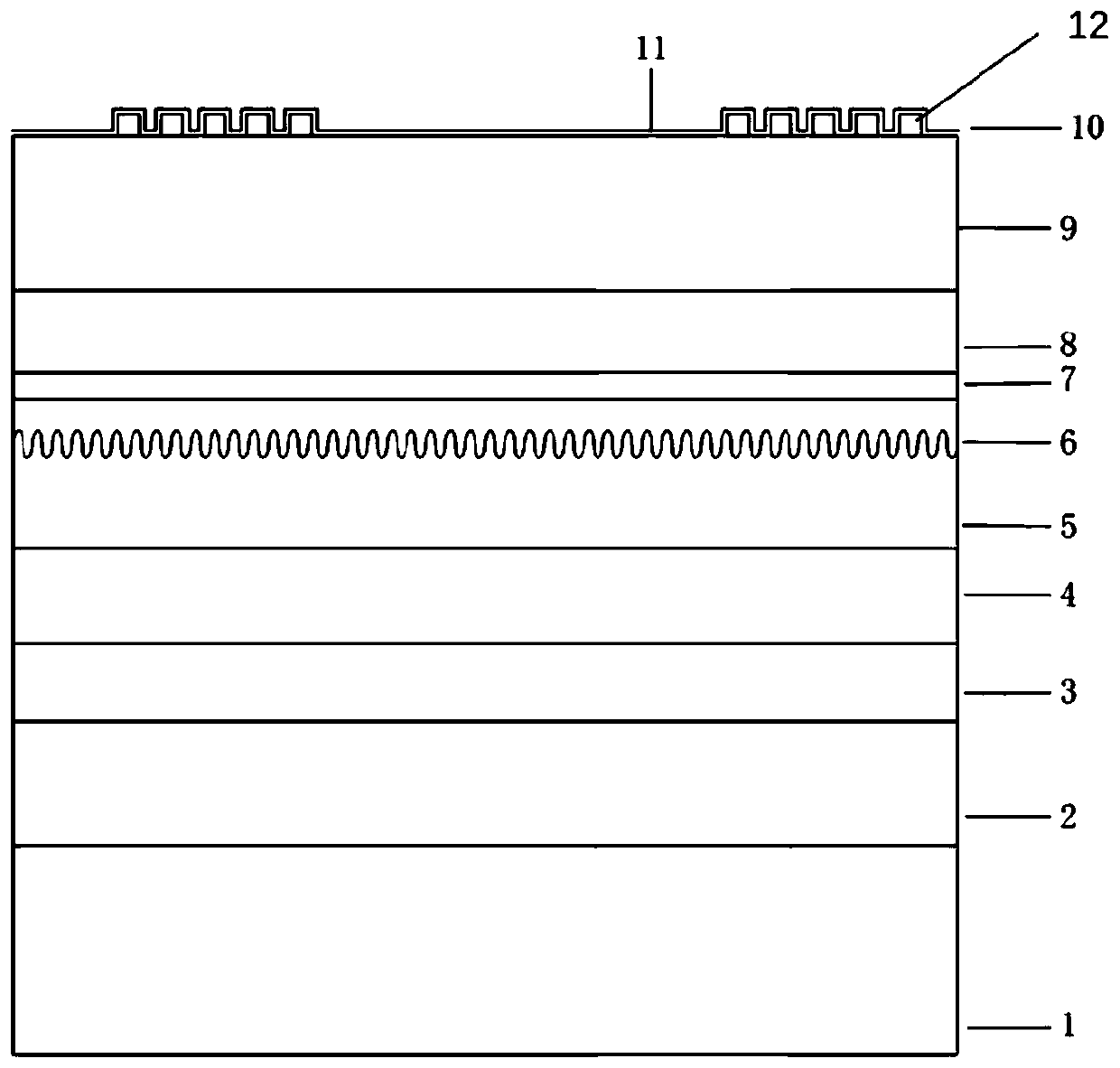
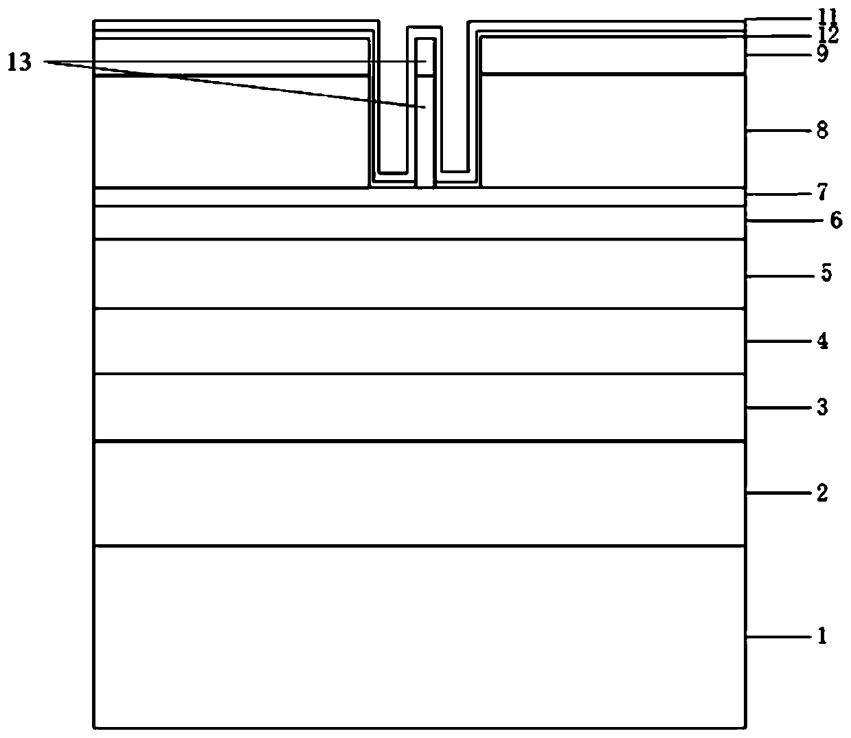
[0041] The invention proposes a feedback semiconductor laser with narrow line width distribution and a two-layer grating structure. The distributed feedback grating includes a secondary epitaxial distributed feedback grating near the active area and an electrode sampling grating composed of periodic ohmic contacts of electrodes. Specifically, the chip structure of the laser includes an N-face electrode layer, a substrate layer, a buffer layer, a lower waveguide layer, an active layer, an upper waveguide layer, a secondary epitaxial grating layer, an etching self-stop layer, and a cladding layer from bottom to top. layer, ohmic contact layer, passivation layer and P-side electrode layer. The cladding layer and the ohmic contact layer form a waveguide structure, and the waveguide structure is a ridge waveguide structure, and the grating structure of the laser includes a secondary epitaxial grating and an electrode sampling grating. The light-emitting surface of the laser has an...


PUM

PropertyMeasurementUnit
Thicknessaaaaaaaaaa
Thicknessaaaaaaaaaa
Thicknessaaaaaaaaaa

Abstract

The invention provides a distributed feedback semiconductor laser which sequentially comprises an N-surface electrode layer, a substrate layer, a buffer layer, a lower waveguide layer, an active layer, an upper waveguide layer, a secondary epitaxial grating layer, an etching self-stop layer, a cladding layer, an ohmic contact layer, a passivation layer and a P-surface electrode layer from bottom to top. The cladding layer and the ohmic contact layer form a waveguide structure, and the waveguide structure is a ridge waveguide structure. An upper grating structure and a lower grating structure in the vertical direction are used for jointly feeding back mode selection. Secondary epitaxial gratings distributed near the active region are efficiently coupled with a light field so that frequencyselection and line width reduction are realized. The single reflection peak line width of the electrode sampling grating is narrow, the electrode sampling grating is fully coupled with a light field in the waveguide for feedback, the working wavelength can be further stabilized, the side-mode rejection ratio is improved, the line width factor is reduced and the laser line width is effectively narrowed.

Description

technical field [0001] The invention relates to the technical field of semiconductor lasers, in particular to a narrow line width distribution feedback semiconductor laser and a preparation method thereof. Background technique [0002] Narrow linewidth lasers have very broad application prospects in coherent optical communications, lidar, dense wavelength division multiplexing, optical fiber sensing, precision optical measurement, holography and other fields. With the rapid development of optical communication networks and smart travel in recent years, the demand for narrow linewidth lasers has become increasingly prominent. Among them, narrow linewidth semiconductor lasers have the advantages of small size, light weight, high efficiency, long life, direct current drive, narrow spectral linewidth, and good coherence, and become ideal light sources for single longitudinal mode, stable wavelength, and narrow linewidth lasers. . [0003] Narrow linewidth semiconductor lasers ...

Claims


Application Information

Patent Timeline
IPC IPC(8): H01S5/12H01S5/22
CPCH01S5/12H01S5/1228H01S5/22
Inventor 孙甲政许博蕊孙文惠夏施君袁海庆祝宁华班德超刘泽秋张晨炜徐长达
Owner INST OF SEMICONDUCTORS - CHINESE ACAD OF SCI
Why Eureka
Try Eureka